SLLS646C March 2008 – June 2017 TL16C752C
PRODUCTION DATA.
- 1 Features
- 2 Applications
- 3 Description
- 4 Revision History
- 5 Description (continued)
- 6 Pin Configuration and Functions
- 7 Specifications
-
8 Detailed Description
- 8.1 Overview
- 8.2 Functional Block Diagram
- 8.3
Feature Description
- 8.3.1
Functional Description
- 8.3.1.1 Trigger Levels
- 8.3.1.2 Hardware Flow Control
- 8.3.1.3 Auto-RTS
- 8.3.1.4 Auto-CTS
- 8.3.1.5 Software Flow Control
- 8.3.1.6 Software Flow Control Example
- 8.3.1.7 Reset
- 8.3.1.8 Interrupts
- 8.3.1.9 Interrupt Mode Operation
- 8.3.1.10 Polled Mode Operation
- 8.3.1.11 Break and Timeout Conditions
- 8.3.1.12 Programmable Baud Rate Generator
- 8.3.1
Functional Description
- 8.4 Device Functional Modes
- 8.5
Register Maps
- 8.5.1 Principals of Operation
- 8.5.2 Receiver Holding Register (RHR)
- 8.5.3 Transmit Holding Register (THR)
- 8.5.4 FIFO Control Register (FCR)
- 8.5.5 Line Control Register (LCR)
- 8.5.6 Line Status Register (LSR)
- 8.5.7 Modem Control Register (MCR)
- 8.5.8 Modem Status Register (MSR)
- 8.5.9 Interrupt Enable Register (IER)
- 8.5.10 Interrupt Identification Register (IIR)
- 8.5.11 Enhanced Feature Register (EFR)
- 8.5.12 Divisor Latches (DLL, DLH)
- 8.5.13 Transmission Control Register (TCR)
- 8.5.14 Trigger Level Register (TLR)
- 8.5.15 FIFO Ready Register
- 8.5.16 Alternate Function Register (AFR)
- 8.5.17 RS-485 Mode
- 8.5.18 IrDA Overview
- 8.5.19 IrDA Encoder Function
- 9 Application and Implementation
- 10Power Supply Recommendations
- 11Layout
- 12Device and Documentation Support
- 13Mechanical, Packaging, and Orderable Information
Package Options
Mechanical Data (Package|Pins)
Thermal pad, mechanical data (Package|Pins)
- RHB|32
Orderable Information
1 Features
- SC16C752B and XR16M752 Pin Compatible With Additional Enhancements
- Support 1.8-V, 2.5-V, 3.3-V, or 5-V Supply
- Characterized for Operation from –40°C to 85°C
- Supports up to:
- 48-MHz Oscillator Input Clock (3 Mbps) for 5-V Operation
- 32-MHz Oscillator Input Clock (2 Mbps) for 3.3-V Operation
- 24-MHz Input Clock (1.5 Mbps) for 2.5-V Operation
- 16-MHz Input Clock (1 Mbps) for 1.8-V Operation
- 64-Byte Transmit/Receive FIFO
- Software-Selectable Baud-Rate Generator
- Programmable and Selectable Transmit and Receive FIFO Trigger Levels for DMA, Interrupt Generation, and Software or Hardware Flow Control
- Software/Hardware Flow Control
- Programmable Xon and Xoff Characters With Optional Xon Any Character
- Programmable Auto-RTS and Auto-CTS-Modem Control Functions (CTS, RTS, DSR, DTR, RI, and CD)
- DMA Signaling Capability for Both Received and Transmitted Data on PN Package
- RS-485 Mode Support
- Infrared Data Association (IrDA) Capability
- Programmable Sleep Mode
- Programmable Serial Interface Characteristics
- 5, 6, 7, or 8-Bit Characters With 1, 1.5, or 2 Stop Bit Generation
- Even, Odd, or No Parity Bit Generation and Detection
- False Start Bit and Line Break Detection
- Internal Test and Loopback Capabilities
2 Applications
- GPS Systems
- Ethernet Network Routers
- Infrared Transceivers
- Domestic Applications
- Portable Applications
- Factory Automation and Process Control
3 Description
The TL16C752C is a dual universal asynchronous receiver transmitter (UART) with 64-byte FIFOs, automatic hardware and software flow control, and data rates up to 3 Mbps. The device offers enhanced features. It has a transmission Character control register (TCR) that stores received FIFO threshold level to start or stop transmission during hardware and software flow control.
Device Information(1)
| PART NUMBER | PACKAGE | BODY SIZE (NOM) |
|---|---|---|
| TL16C752C | TQFP (48) | 7.00 mm × 7.00 mm |
| VQFN (32) | 5.00 mm x 5.00 mm |
- For all available packages, see the orderable addendum at the end of the data sheet.
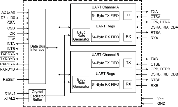
Block Diagram
