SLVS719G June 2008 – January 2015 TL1963A
PRODUCTION DATA.
- 1 Features
- 2 Applications
- 3 Description
- 4 Revision History
- 5 Description (continued)
- 6 Device Comparison Table
- 7 Pin Configuration and Functions
- 8 Specifications
- 9 Detailed Description
- 10Application and Implementation
- 11Power Supply Recommendations
- 12Layout
- 13Device and Documentation Support
- 14Mechanical, Packaging, and Orderable Information
Package Options
Mechanical Data (Package|Pins)
Thermal pad, mechanical data (Package|Pins)
Orderable Information
12 Layout
12.1 Layout Guidelines
- For best performance, all traces should be as short as possible.
- Use wide traces for IN, OUT, and GND to minimize the parasitic electrical effects.
- A minimum output capacitor of 10 μF with an ESR of 3 Ω or less is recommended to prevent oscillations. X5R and X7R dielectrics are preferred.
- Place the Output Capacitor as close as possible to the OUT pin of the device.
- The tab of the DCQ package should be connected to ground.
- The exposed thermal pad of the KTT package should be connected to a wide ground plane for effective heat dissipation.
12.2 Layout Example
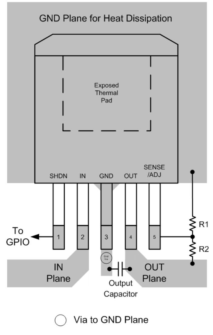 Figure 36. TO-263 Layout Example (KTT)
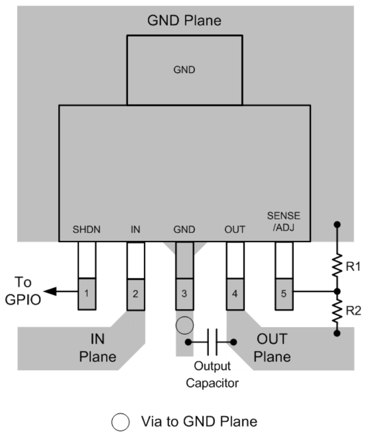 Figure 37. 6SOT-223 Layout Example (DCQ)
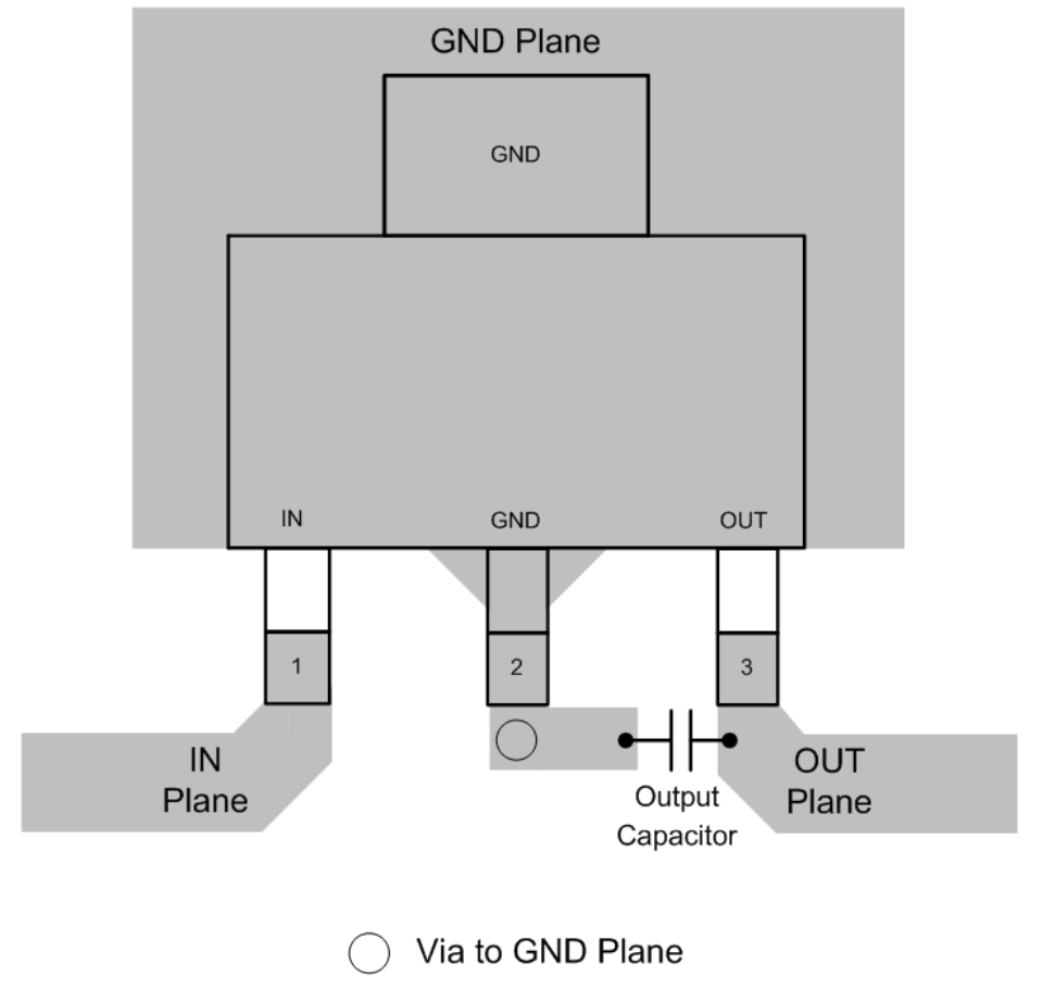 Figure 38. 4SOT-223 Layout Example (DCY)
12.3 Thermal Considerations
The power handling capability of the device is limited by the recommended maximum operating junction temperature (125°C). The power dissipated by the device is made up of two components:
- Output current multiplied by the input/output voltage differential: IOUT(VIN – VOUT)
- GND pin current multiplied by the input voltage: IGNDVIN
The GND pin current can be found using the GND Pin Current graphs in Typical Characteristics. Power dissipation is equal to the sum of the two components listed above.
The TL1963A-xx series regulators have internal thermal limiting designed to protect the device during overload conditions. For continuous normal conditions, the recommended maximum operating junction temperature is 125 °C. It is important to give careful consideration to all sources of thermal resistance from junction to ambient. Additional heat sources mounted nearby must also be considered.
For surface-mount devices, heat sinking is accomplished by using the heat-spreading capabilities of the PC board and its copper traces. Copper board stiffeners and plated through-holes can also be used to spread the heat generated by power devices.
Table 4 lists thermal resistance for several different board sizes and copper areas. All measurements were taken in still air on 1/16" FR-4 board with 1-oz copper.
Table 4. Thermal Data for KTT Package (5-Pin TO-263)
| COPPER AREA | BOARD AREA | THERMAL RESISTANCE (JUNCTION TO AMBIENT) |
|
|---|---|---|---|
| TOPSIDE(1) | BACKSIDE | ||
| 2500 mm2 | 2500 mm2 | 2500 mm2 | 23°C/W |
| 1000 mm2 | 2500 mm2 | 2500 mm2 | 25°C/W |
| 125 mm2 | 2500 mm2 | 2500 mm2 | 33°C/W |
12.3.1 Calculating Junction Temperature
Example: Given an output voltage of 3.3 V, an input voltage range of 4 V to 6 V, an output current range of 0 mA to 500 mA, and a maximum ambient temperature of 50°C, what is the operating junction temperature?
The power dissipated by the device is equal to:
where
- IOUT(MAX) = 500 mA
- VIN(MAX) = 6 V
- IGND at (IOUT = 500 mA, VIN = 6 V) = 10 mA
So,
Using a KTT package, the thermal resistance is in the range of 23°C/W to 33°C/W, depending on the copper area. So the junction temperature rise above ambient is approximately equal to:
The junction temperature rise can then be added to the maximum ambient temperature to find the operating junction temperature (TJ):