SLVS038I January 1989 – July 2016 TL2842 , TL2843 , TL2844 , TL2845 , TL3842 , TL3843 , TL3844 , TL3845
PRODUCTION DATA.
- 1 Features
- 2 Applications
- 3 Description
- 4 Revision History
- 5 Pin Configuration and Functions
- 6 Specifications
- 7 Detailed Description
- 8 Application and Implementation
- 9 Power Supply Recommendations
- 10Layout
- 11Device and Documentation Support
- 12Mechanical, Packaging, and Orderable Information
Package Options
Refer to the PDF data sheet for device specific package drawings
Mechanical Data (Package|Pins)
- D|14
- D|8
- P|8
Thermal pad, mechanical data (Package|Pins)
Orderable Information
10 Layout
10.1 Layout Guidelines
Always try to use a low EMI inductor with a ferrite type closed core. Some examples would be toroid and encased E core inductors. Open core can be used if they have low EMI characteristics and are located a bit more away from the low power traces and components. Make the poles perpendicular to the PCB as well if using an open core. Stick cores usually emit the most unwanted noise.
10.1.1 Feedback Traces
Try to run the feedback trace as far from the inductor and noisy power traces as possible. Also, keep the feedback trace to be as direct as possible and somewhat thick. These two sometimes involve a trade-off, but keeping it away from inductor EMI and other noise sources is the more critical of the two. Run the feedback trace on the side of the PCB opposite of the inductor with a ground plane separating the two.
10.1.2 Input/Output Capacitors
When using a low value ceramic input filter capacitor, it should be located as close to the VCC pin of the IC as possible. This will eliminate as much trace inductance effects as possible and give the internal IC rail a cleaner voltage supply. Some designs require the use of a feed-forward capacitor connected from the output to the feedback pin as well, usually for stability reasons. In this case it should also be positioned as close to the IC as possible. Using surface mount capacitors also reduces lead length and lessens the chance of noise coupling into the effective antenna created by through-hole components.
10.1.3 Compensation Components
External compensation components for stability should also be placed close to the IC. Surface mount components are recommended here as well for the same reasons discussed for the filter capacitors. These should not be located very close to the inductor either.
10.1.4 Traces and Ground Planes
Make all of the power (high current) traces as short, direct, and thick as possible. It is good practice on a standard PCB board to make the traces an absolute minimum of 15 mils (0.381 mm) per Ampere. The inductor, output capacitors, and output diode should be as close to each other possible. This helps reduce the EMI radiated by the power traces due to the high switching currents through them. This will also reduce lead inductance and resistance as well, which in turn reduces noise spikes, ringing, and resistive losses that produce voltage errors.
The grounds of the IC, input capacitors, output capacitors, and output diode (if applicable) should be connected close together directly to a ground plane. It would also be a good idea to have a ground plane on both sides of the PCB. This will reduce noise as well by reducing ground loop errors as well as by absorbing more of the EMI radiated by the inductor. For multi-layer boards with more than two layers, a ground plane can be used to separate the power plane (where the power traces and components are) and the signal plane (where the feedback and compensation and components are) for improved performance. On multi-layer boards the use of vias will be required to connect traces and different planes. It is good practice to use one standard via per 200 mA of current if the trace will need to conduct a significant amount of current from one plane to the other.
Arrange the components so that the switching current loops curl in the same direction. Due to the way switching regulators operate, there are two power states. One state when the switch is on and one when the switch is off. During each state there will be a current loop made by the power components that are currently conducting. Place the power components so that during each of the two states the current loop is conducting in the same direction. This prevents magnetic field reversal caused by the traces between the two half-cycles and reduces radiated EMI.
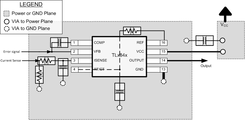
10.2 Layout Example
 Figure 18. Layout of D-8 or P Package for TLx84x Devices