SLOS467H October 2006 – January 2015 TL971 , TL972 , TL974
PRODUCTION DATA.
- 1 Features
- 2 Applications
- 3 Description
- 4 Simplified Schematic
- 5 Revision History
- 6 Pin Configuration and Functions
- 7 Specifications
- 8 Detailed Description
- 9 Application and Implementation
- 10Power Supply Recommendations
- 11Layout
- 12Device and Documentation Support
- 13Mechanical, Packaging, and Orderable Information
Package Options
Refer to the PDF data sheet for device specific package drawings
Mechanical Data (Package|Pins)
- D|8
Thermal pad, mechanical data (Package|Pins)
Orderable Information
9 Application and Implementation
NOTE
Information in the following applications sections is not part of the TI component specification, and TI does not warrant its accuracy or completeness. TI’s customers are responsible for determining suitability of components for their purposes. Customers should validate and test their design implementation to confirm system functionality.
9.1 Typical Application
The voltage follower configuration of the operational amplifier is used for applications where a weak signal is used to drive a relatively high current load. This circuit is also called a buffer amplifier or unity gain amplifier. The inputs of an operational amplifier have a very high resistance which puts a negligible current load on the voltage source. The output resistance of the operational amplifier is almost negligible, so it can provide as much current as necessary to the output load.
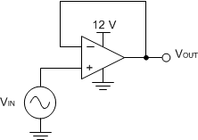 Figure 17. Voltage follower schematic
9.1.1 Design Requirements
- Input at positive Terminal
- Output range of 0 V to 12 V
- Input range of 0 V to 12 V
- Short-circuit feedback to negative input for unity gain
9.1.2 Detailed Design Procedure
9.1.2.1 Output Voltage Swing
The output voltage of an operational amplifier is limited by its internal circuitry to some level below the supply rails. For this amplifier, the output voltage must be within ±12 V.
9.1.2.2 Supply and Input Voltage
For correct operation of the amplifier, neither input must be higher than the recommended positive supply rail voltage or lower than the recommended negative supply rail voltage. The chosen amplifier must be able to operate at the supply voltage that accommodates the inputs. Because the input for this application goes up to 12 V, the supply voltage must be 15 V. Using a negative voltage on the lower rail rather than ground, allows the amplifier to maintain linearity for the full range of inputs.
9.1.3 Application Curves for Output Characteristics
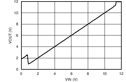 Figure 18. Output Voltage vs Input Voltage
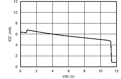 Figure 20. Current Dawn from Supply (ICC)
vs Input Voltage
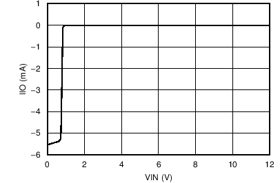 Figure 19. Current Drawn by Input of Voltage Follower (IIO)
vs Input Voltage