SBAS846 November 2017 TLA2021 , TLA2022 , TLA2024
PRODUCTION DATA.
- 1 Features
- 2 Applications
- 3 Description
- 4 Revision History
- 5 Device Comparison Table
- 6 Pin Configuration and Functions
- 7 Specifications
- 8 Detailed Description
- 9 Register Maps
- 10Application and Implementation
- 11Power Supply Recommendations
- 12Layout
- 13Device and Documentation Support
- 14Mechanical, Packaging, and Orderable Information
Package Options
Mechanical Data (Package|Pins)
- RUG|10
Thermal pad, mechanical data (Package|Pins)
Orderable Information
7 Specifications
7.1 Absolute Maximum Ratings(1)
| MIN | MAX | UNIT | ||
|---|---|---|---|---|
| Power-supply voltage | VDD to GND | –0.3 | 7 | V |
| Analog input voltage | AIN0, AIN1, AIN2, AIN3 | GND – 0.3 | VDD + 0.3 | |
| Digital input voltage | SDA, SCL, ADDR | GND – 0.3 | 7 | |
| Input current | Continuous, any pin except power-supply pins | –10 | 10 | mA |
| Temperature | Junction, TJ | –40 | 125 | °C |
| Storage, Tstg | –60 | 125 | ||
(1) Stresses beyond those listed under Absolute Maximum Ratings may cause permanent damage to the device. These are stress ratings only, which do not imply functional operation of the device at these or any other conditions beyond those indicated under Recommended Operating Conditions. Exposure to absolute-maximum-rated conditions for extended periods may affect device reliability.
7.2 ESD Ratings
| VALUE | UNIT | |||
|---|---|---|---|---|
| V(ESD) | Electrostatic discharge | Human-body model (HBM), per ANSI/ESDA/JEDEC JS-001(1) | ±2000 | V |
| Charged-device model (CDM), per JEDEC specification JESD22-C101(2) | ±500 | |||
(1) JEDEC document JEP155 states that 500-V HBM allows safe manufacturing with a standard ESD control process.
(2) JEDEC document JEP157 states that 250-V CDM allows safe manufacturing with a standard ESD control process.
7.3 Recommended Operating Conditions
over operating ambient temperature range (unless otherwise noted)| MIN | NOM | MAX | UNIT | ||
|---|---|---|---|---|---|
| POWER SUPPLY | |||||
| VDD to GND | 2 | 5.5 | V | ||
| ANALOG INPUTS(1) | |||||
| FSR | Full-scale input voltage range(2)
(VIN = VAINP – VAINN) |
±0.256 | ±6.144 | V | |
| V(AINx) | Absolute input voltage | GND | VDD | V | |
| DIGITAL INPUTS | |||||
| Digital input voltage | GND | 5.5 | V | ||
| TEMPERATURE | |||||
| TA | Operating ambient temperature | –40 | 85 | °C | |
(1) AINP and AINN denote the selected positive and negative inputs. On the TLA2024, AINx denotes one of the four available analog inputs.
(2) This parameter expresses the full-scale range of the ADC scaling. No more than VDD + 0.3 V or 5.5 V (whichever is smaller) must be applied to this device. See the Full-Scale Range (FSR) and LSB Size section more information.
7.4 Thermal Information
| THERMAL METRIC(1) | TLA202x | UNIT | |
|---|---|---|---|
| RUG (X2QFN) | |||
| 10 PINS | |||
| RθJA | Junction-to-ambient thermal resistance | 245.2 | °C/W |
| RθJC(top) | Junction-to-case (top) thermal resistance | 69.3 | °C/W |
| RθJB | Junction-to-board thermal resistance | 172.0 | °C/W |
| ψJT | Junction-to-top characterization parameter | 8.2 | °C/W |
| ψJB | Junction-to-board characterization parameter | 170.8 | °C/W |
| RθJC(bot) | Junction-to-case (bottom) thermal resistance | N/A | °C/W |
(1) For more information about traditional and new thermal metrics, see the Semiconductor and IC Package Thermal Metrics application report.
7.5 Electrical Characteristics
minimum and maximum specifications apply from TA = –40°C to +85°C; typical specifications are at TA = 25°C; all specifications are at VDD = 3.3 V, data rate = 128 SPS, and FSR = ±2.048 V (unless otherwise noted)| PARAMETER | TEST CONDITIONS | MIN | TYP | MAX | UNIT | |
|---|---|---|---|---|---|---|
| ANALOG INPUT | ||||||
| Common-mode input impedance | FSR = ±6.144 V(1) | 10 | MΩ | |||
| FSR = ±4.096 V(1), FSR = ±2.048 V | 6 | |||||
| FSR = ±1.024 V | 3 | |||||
| FSR = ±0.512 V, FSR = ±0.256 V | 100 | |||||
| Differential input impedance | FSR = ±6.144 V(1) | 22 | MΩ | |||
| FSR = ±4.096 V(1) | 15 | |||||
| FSR = ±2.048 V | 4.9 | |||||
| FSR = ±1.024 V | 2.4 | |||||
| FSR = ±0.512 V, ±0.256 V | 710 | kΩ | ||||
| SYSTEM PERFORMANCE | ||||||
| Resolution (no missing codes) | 12 | Bits | ||||
| DR | Data rate | 128, 250, 490, 920, 1600, 2400, 3300 | SPS | |||
| Data rate variation | All data rates | –10% | 10% | |||
| INL | Integral nonlinearity(2) | 1 | LSB | |||
| Offset error | ±1 | LSB | ||||
| Offset drift | 0.01 | LSB/°C | ||||
| Gain error(3) | 0.05% | |||||
| Gain drift(3) | 10 | ppm/°C | ||||
| PSRR | Power-supply rejection ratio | 85 | dB | |||
| CMRR | Common-mode rejection ratio | 90 | dB | |||
| DIGITAL INPUT/OUTPUT | ||||||
| VIL | Logic input level, low | GND | 0.3 VDD | V | ||
| VIH | Logic input level, high | 0.7 VDD | 5.5 | V | ||
| VOL | Logic output level, low | IOL = 3 mA | GND | 0.15 | 0.4 | V |
| Input leakage current | GND < VDigital Input < VDD | –10 | 10 | µA | ||
| POWER SUPPLY | ||||||
| IVDD | Supply current | Power-down | 0.5 | µA | ||
| Operating | 150 | |||||
| PD | Power dissipation | VDD = 5 V | 0.9 | mW | ||
| VDD = 3.3 V | 0.5 | |||||
| VDD = 2 V | 0.3 | |||||
(1) This parameter expresses the full-scale range of the ADC scaling. No more than VDD + 0.3 V or 5.5 V (whichever is smaller) must be applied to this device. See the Full-Scale Range (FSR) and LSB Size section for more information.
(2) Best-fit INL; covers 99% of full-scale.
(3) Includes all errors from onboard PGA and voltage reference.
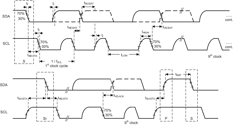
7.6 I2C Timing Requirements
over operating ambient temperature range and VDD = 2 V to 5.5 V (unless otherwise noted)| MIN | MAX | UNIT | |||
|---|---|---|---|---|---|
| STANDARD-MODE | |||||
| fSCL | SCL clock frequency | 10 | 100 | kHz | |
| tLOW | Pulse duration, SCL low | 4.7 | µs | ||
| tHIGH | Pulse duration, SCL high | 4.0 | µs | ||
| tHD;STA | Hold time, (repeated) START condition. After this period, the first clock pulse is generated. |
4 | µs | ||
| tSU;STA | Setup time, repeated START condition | 4.7 | µs | ||
| tHD;DAT | Hold time, data | 0 | µs | ||
| tSU;DAT | Setup time, data | 250 | ns | ||
| tr | Rise time, SCL, SDA | 1000 | ns | ||
| tf | Fall time, SCL, SDA | 250 | ns | ||
| tSU;STO | Setup time, STOP condition | 4.0 | µs | ||
| tBUF | Bus free time, between STOP and START condition | 4.7 | µs | ||
| tVD;DAT | Valid time, data | 3.45 | µs | ||
| tVD;ACK | Valid time, acknowledge | 3.45 | µs | ||
| FAST-MODE | |||||
| fSCL | SCL clock frequency | 10 | 400 | kHz | |
| tLOW | Pulse duration, SCL low | 1.3 | µs | ||
| tHIGH | Pulse duration, SCL high | 0.6 | µs | ||
| tHD;STA | Hold time, (repeated) START condition. After this period, the first clock pulse is generated. |
0.6 | µs | ||
| tSU;STA | Setup time, repeated START condition | 0.6 | µs | ||
| tHD;DAT | Hold time, data | 0 | µs | ||
| tSU;DAT | Setup time, data | 100 | ns | ||
| tr | Rise time, SCL, SDA | 20 | 300 | ns | |
| tf | Fall time, SCL, SDA | 300 | ns | ||
| tSU;STO | Setup time, STOP condition | 0.6 | µs | ||
| tBUF | Bus free time, between STOP and START condition | 1.3 | µs | ||
| tVD;DAT | Valid time, data | 0.9 | µs | ||
| tVD;ACK | Valid time, acknowledge | 0.9 | µs | ||
 Figure 1. I2C Timing Requirements
7.7 Typical Characteristics
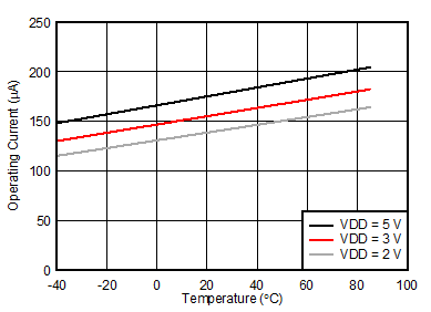
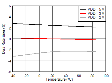
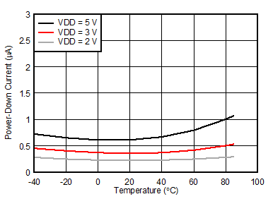
at FSR = ±2.048 V and DR = 128 SPS (unless otherwise noted)

