SLVS934C June 2009 – February 2021 TLC59025
PRODUCTION DATA
- 1 Features
- 2 Applications
- 3 Description
- 4 Revision History
- 5 Pin Configuration and Functions
-
6 Specifications
- 6.1 Absolute Maximum Ratings
- 6.2 ESD Ratings
- 6.3 Recommended Operating Conditions
- 6.4 Thermal Information
- 6.5 Electrical Characteristics for 3-V Input Voltage
- 6.6 Electrical Characteristics for 5.5-V Input Voltage
- 6.7 Power Dissipation Ratings
- 6.8 Timing Requirements
- 6.9 Switching Characteristics for 3-V Input Voltage
- 6.10 Switching Characteristics for 5.5-V Input Voltage
- 6.11 Typical Characteristics
- 7 Parameter Measurement Information
- 8 Detailed Description
- 9 Application and Implementation
- 10Power Supply Recommendations
- 11Layout
- 12Device and Documentation Support
- 13Mechanical, Packaging, and Orderable Information
Package Options
Mechanical Data (Package|Pins)
- DBQ|24
Thermal pad, mechanical data (Package|Pins)
Orderable Information
6.8 Timing Requirements
VDD = 3 V to 5.5 V (unless otherwise noted)
| MIN | MAX | UNIT | |||
|---|---|---|---|---|---|
| tw(L) | LE pulse duration | 15 | ns | ||
| tw(CLK) | CLK pulse duration | 15 | ns | ||
| tw(OE) | OE pulse duration | 300 | ns | ||
| tsu(D) | Setup time for SDI | 3 | ns | ||
| th(D) | Hold time for SDI | 2 | ns | ||
| tsu(L) | Setup time for LE | 5 | ns | ||
| th(L) | Hold time for LE | 5 | ns | ||
| fCLK | Clock frequency | Cascade operation | 30 | MHz | |
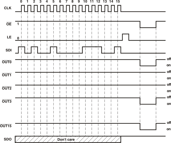
 Figure 6-1 Timing Diagram