SLDS162B March 2009 – December 2015 TLC59108F
PRODUCTION DATA.
- 1 Features
- 2 Applications
- 3 Description
- 4 Revision History
- 5 Pin Configuration and Functions
- 6 Specifications
- 7 Parameter Measurement Information
-
8 Detailed Description
- 8.1 Overview
- 8.2 Functional Block Diagram
- 8.3 Feature Description
- 8.4 Device Functional Modes
- 8.5 Programming
- 8.6
Register Maps
- 8.6.1 Control Register
- 8.6.2 Mode Register 1 (MODE1)
- 8.6.3 Mode Register 2 (MODE2)
- 8.6.4 Individual Brightness Control Registers (PWM0-PWM7)
- 8.6.5 Group Duty Cycle Control Register (GRPPWM)
- 8.6.6 Group Frequency Register (GRPFREQ)
- 8.6.7 LED Driver Output State Registers (LEDOUT0, LEDOUT1)
- 8.6.8 I2C Bus Sub-Address Registers 1 to 3 (SUBADR1-SUBADR3)
- 8.6.9 LED All Call I2C Bus Address Register (ALLCALLADR)
- 9 Application and Implementation
- 10Power Supply Recommendations
- 11Layout
- 12Device and Documentation Support
- 13Mechanical, Packaging, and Orderable Information
Package Options
Mechanical Data (Package|Pins)
- PW|20
Thermal pad, mechanical data (Package|Pins)
Orderable Information
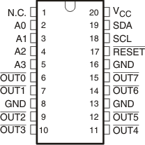
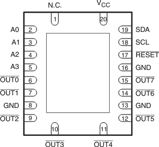
5 Pin Configuration and Functions
PW Package
20-Pin TSSOP
Top View

N.C. – No internal connection
RGY Package
20-Pin VQFN With Exposed Thermal Pad
Top View

Pin Functions
| PIN | I/O(1) | DESCRIPTION | |
|---|---|---|---|
| NAME | NO. | ||
| A0 | 2 | I | Address input 0 |
| A1 | 3 | I | Address input 1 |
| A2 | 4 | I | Address input 2 |
| A3 | 5 | I | Address input 3 |
| GND | 8 | – | Ground |
| 13 | |||
| 16 | |||
| N.C. | 1 | I | No internal connection |
| OUT0 | 6 | O | Open-drain output 0 to 7, LED ON at low |
| OUT1 | 7 | ||
| OUT2 | 9 | ||
| OUT3 | 10 | ||
| OUT4 | 11 | ||
| OUT5 | 12 | ||
| OUT6 | 14 | ||
| OUT7 | 15 | ||
| RESET | 17 | I | Active-low reset input |
| SCL | 18 | I | Serial clock input |
| SDA | 19 | I/O | Serial data input/output |
| VCC | 20 | – | Power supply |
(1) I = input, O = output