SLDS157E February 2008 – December 2014 TLC59116
PRODUCTION DATA.
- 1 Features
- 2 Applications
- 3 Description
- 4 Revision History
- 5 Description (continued)
- 6 Pin Configuration and Functions
- 7 Specifications
- 8 Parameter Measurement Information
-
9 Detailed Description
- 9.1 Overview
- 9.2 Functional Block Diagram
- 9.3 Feature Description
- 9.4 Device Functional Modes
- 9.5
Register Maps
- 9.5.1 Mode Register 1 (MODE1)"SLEEP" to "OSC" in Mode Register 1 (MODE1) Table.
- 9.5.2 Mode Register 2 (MODE2)
- 9.5.3 Brightness Control Registers 0 to 15 (PWM0 to PWM15)
- 9.5.4 Group Duty Cycle Control Register (GRPPWM)
- 9.5.5 Group Frequency Register (GRPFREQ)
- 9.5.6 LED Driver Output State Registers 0 to 3 (LEDOUT0 to LEDOUT3)
- 9.5.7 I2C Bus Subaddress Registers 1 to 3 (SUBADR1 to SUBADR3)
- 9.5.8 LED All Call I2C Bus Address Register (ALLCALLADR)
- 9.5.9 Output Gain Control Register (IREF)
- 9.5.10 Error Flags Registers (EFLAG1, EFLAG2)
- 9.5.11 Control Register
-
10Application and Implementation
- 10.1 Application Information
- 10.2 Typical Application
- 11Power Supply Recommendations
- 12Layout
- 13Device and Documentation Support
- 14Mechanical, Packaging, and Orderable Information
Package Options
Mechanical Data (Package|Pins)
Thermal pad, mechanical data (Package|Pins)
- RHB|32
Orderable Information
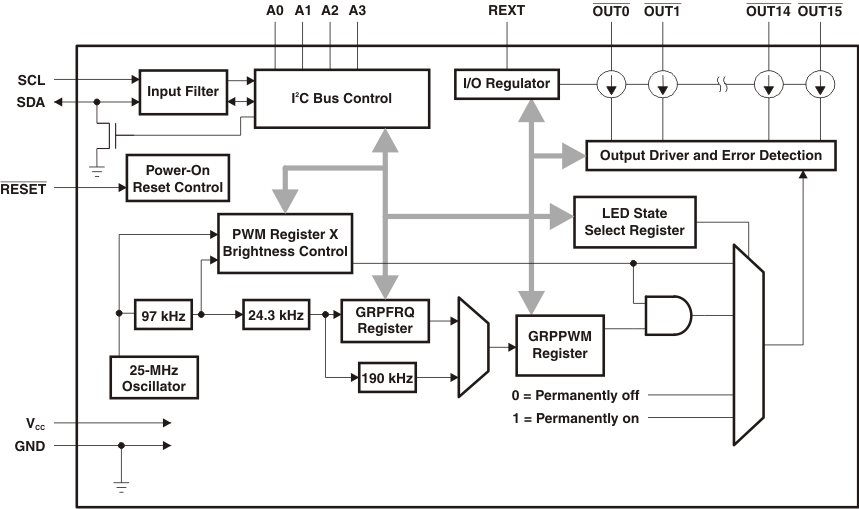
9 Detailed Description
9.1 Overview
The TLC59116 is an I2C bus controlled 16-channel LED driver that is optimized for red/green/blue/amber (RGBA) color mixing and backlight application. Each LED output has its own 8-bit resolution (256 steps) fixed-frequency individual PWM controller that operates at 97 kHz, with a duty cycle that is adjustable from 0% to 99.6%. The individual PWM controller allows each LED to be set to a specific brightness value. An additional 8-bit resolution (256 steps) group PWM controller has both a fixed frequency of 190 Hz and an adjustable frequency between 24 Hz to once every 10.73 seconds, with a duty cycle that is adjustable from 0% to 99.6%. The group PWM controller dims or blinks all LEDs with the same value.
9.2 Functional Block Diagram
9.3 Feature Description
9.3.1 Open-Circuit Detection
The TLC59116 LED open-circuit detection compares the effective current level IOUT with the open load detection threshold current IOUT,Th. If IOUT is below the threshold IOUT,Th the TLC59116 detects an open load condition. This error status can be read out as an error flag through the registers EFLAG1 and EFLAG2.
For open-circuit error detection, a channel must be on and the PWM must be off.
9.3.2 Overtemperature Detection and Shutdown
The TLC59116 LED is equipped with a global overtemperature sensor and 16 individual channel-selective overtemperature sensors.
- When the global sensor reaches the trip temperature, all output channels are shut down, and the error status is stored in the internal Error Status register of every channel. After shutdown, the channels automatically restart after cooling down, if the control signal (output latch) remains on. The stored error status is not reset after cooling down and can be read out as the error status code in registers EFLAG1 and EFLAG2.
- When one of the channel-specific sensors reaches trip temperature, only the affected output channel is shut down, and the error status is stored only in the internal Error Status register of the affected channel. After shutdown, the channel automatically restarts after cooling down, if the control signal (output latch) remains on. The stored error status is not reset after cooling down and can be read out as error status code in registers EFLAG1 and EFLAG2.
For channel-specific overtemperature error detection, a channel must be on.
The error flags of open-circuit and overtemperature are ORed to set the EFLAG1 and EFLAG2 registers.
The error status code due to overtemperature is reset when the host writes 1 to bit 7 of the MODE2 register. The host must write 0 to bit 7 of the MODE2 register to enable the overtemperature error flag.
Table 2. Overtemperature Detection(1)
| STATE OF OUTPUT PORT | CONDITION | ERROR STATUS CODE | MEANING |
|---|---|---|---|
| On On → all channels Off |
Tj < Tj,trip global | 1 | Normal |
| Tj > Tj,trip global | All error status bits = 0 | Global overtemperature | |
| On On → Off |
Tj < Tj,trip channel n | 1 | Normal |
| Tj > Tj,trip channel n | Channel n error status bit = 0 | Channel n overtemperature |
9.3.3 Power-On Reset (POR)
When power is applied to VCC, an internal power-on reset holds the TLC59116 in a reset condition until VCC reaches VPOR. At this point, the reset condition is released and the TLC59116 registers, and I2C bus state machine are initialized to their default states (all zeroes), causing all the channels to be deselected. Thereafter, VCC must be lowered below 0.2 V to reset the device.
9.3.4 External Reset
A reset can be accomplished by holding the RESET pin low for a minimum of tW. The TLC59116 registers and I2C state machine are held in their default states until the RESET input is again high.
This input requires a pullup resistor to VCC if no active connection is used.
9.3.5 Software Reset
The Software Reset Call (SWRST Call) allows all the devices in the I2C bus to be reset to the power-up state value through a specific I2C bus command.
The SWRST Call function is defined as the following:
- A Start command is sent by the I2C bus master.
- The reserved SWRST I2C bus address 1101 011 with the R/W bit set to 0 (write) is sent by the I2C bus master.
- The TLC59116 device(s) acknowledge(s) after seeing the SWRST Call address 1101 0110 (D6h) only. If the R/W bit is set to 1 (read), no acknowledge is returned to the I2C bus master.
- Once the SWRST Call address has been sent and acknowledged, the master sends two bytes with two specific values (SWRST data byte 1 and byte 2):
- Byte1 = A5h: the TLC59116 acknowledges this value only. If byte 1 is not equal to A5h, the TLC59116 does not acknowledge it.
- Byte 2 = 5Ah: the TLC59116 acknowledges this value only. If byte 2 is not equal to 5Ah, the TLC59116 does not acknowledge it.
- Once the correct two bytes (SWRST data byte 1 and byte 2 only) have been sent and correctly acknowledged, the master sends a Stop command to end the SWRST Call. The TLC59116 then resets to the default value (power-up value) and is ready to be addressed again within the specified bus free time (tBUF).
If more than two bytes of data are sent, the TLC59116 does not acknowledge any more.
The I2C bus master may interpret a non-acknowledge from the TLC59116 (at any time) as a SWRST Call Abort. The TLC59116 does not initiate a reset of its registers. This happens only when the format of the Start Call sequence is not correct.
9.3.6 Individual Brightness Control With Group Dimming/Blinking
A 97-kHz fixed-frequency signal with programmable duty cycle (8 bits, 256 steps) is used to control the individual brightness for each LED.
On top of this signal, one of the following signals can be superimposed (this signal can be applied to the four LED outputs):
- A lower 190-Hz fixed-frequency signal with programmable duty cycle (8 bits, 256 steps) provides a global brightness control.
- A programmable frequency signal from 24 Hz to 1/10.73 s (8 bits, 256 steps) provides a global blinking control.
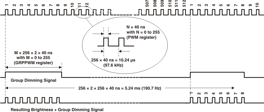
- Minimum pulse width for LEDn brightness control is 40 ns.
- Minimum pulse width for group dimming is 20.48 μs.
- When M = 1 (GRPPWM register value), the resulting LEDn Brightness Control + Group Dimming signal has two pulses of the LED Brightness Control signal (pulse width = n × 40 ns, with n defined in the PWMx register).
- This resulting Brightness + Group Dimming signal shows a resulting control signal with M = 4 (8 pulses).
9.4 Device Functional Modes
9.4.1 Active
Active mode occurs when one or more of the output channels is enabled.
9.4.2 Standby
Standby mode occurs when all output channels are disabled. Standby mode may be entered via I2C command or by pulling the RESET pin low.
9.5 Register Maps
Table 3 describes the registers in the TLC59116.
Table 3. Register Descriptions
| REGISTER NUMBER (HEX) |
NAME | ACCESS(1) | DESCRIPTION |
|---|---|---|---|
| 00 | MODE1 | R/W | Mode 1 |
| 01 | MODE2 | R/W | Mode 2 |
| 02 | PWM0 | R/W | Brightness control LED0 |
| 03 | PWM1 | R/W | Brightness control LED1 |
| 04 | PWM2 | R/W | Brightness control LED2 |
| 05 | PWM3 | R/W | Brightness control LED3 |
| 06 | PWM4 | R/W | Brightness control LED4 |
| 07 | PWM5 | R/W | Brightness control LED5 |
| 08 | PWM6 | R/W | Brightness control LED6 |
| 09 | PWM7 | R/W | Brightness control LED7 |
| 0A | PWM8 | R/W | Brightness control LED8 |
| 0B | PWM9 | R/W | Brightness control LED9 |
| 0C | PWM10 | R/W | Brightness control LED10 |
| 0D | PWM11 | R/W | Brightness control LED11 |
| 0E | PWM12 | R/W | Brightness control LED12 |
| 0F | PWM13 | R/W | Brightness control LED13 |
| 10 | PWM14 | R/W | Brightness control LED14 |
| 11 | PWM15 | R/W | Brightness control LED15 |
| 12 | GRPPWM | R/W | Group duty cycle control |
| 13 | GRPFREQ | R/W | Group frequency |
| 14 | LEDOUT0 | R/W | LED output state 0 |
| 15 | LEDOUT1 | R/W | LED output state 1 |
| 16 | LEDOUT2 | R/W | LED output state 2 |
| 17 | LEDOUT3 | R/W | LED output state 3 |
| 18 | SUBADR1 | R/W | I2C bus subaddress 1 |
| 19 | SUBADR2 | R/W | I2C bus subaddress 2 |
| 1A | SUBADR3 | R/W | I2C bus subaddress 3 |
| 1B | ALLCALLADR | R/W | LED All Call I2C bus address |
| 1C | IREF | R/W | IREF configuration |
| 1D | EFLAG1 | R | Error flags 1 |
| 1E | EFLAG2 | R | Error flags 2 |
9.5.1 Mode Register 1 (MODE1)
Table 4 describes Mode Register 1.
Table 4. MODE1 – Mode Register 1 (Address 00h) Bit Description
| BIT | SYMBOL | ACCESS(1) | VALUE | DESCRIPTION |
|---|---|---|---|---|
| 7 | AI2 | R | 0(2) | Register auto-increment disabled |
| 1 | Register auto-increment enabled | |||
| 6 | AI1 | R | 0(2) | Auto-increment bit 1 = 0 |
| 1 | Auto-increment bit 1 = 1 | |||
| 5 | AI0 | R | 0(2) | Auto-increment bit 0 = 0 |
| 1 | Auto-increment bit 0 = 1 | |||
| 4 | OSC | R/W | 0 | Normal mode(3) |
| 1(2) | Oscillator off. | |||
| 3 | SUB1 | R/W | 0(2) | Device does not respond to I2C bus subaddress 1. |
| 1 | Device responds to I2C bus subaddress 1. | |||
| 2 | SUB2 | R/W | 0(2) | Device does not respond to I2C bus subaddress 2. |
| 1 | Device responds to I2C bus subaddress 2. | |||
| 1 | SUB3 | R/W | 0(2) | Device does not respond to I2C bus subaddress 3. |
| 1 | Device responds to I2C bus subaddress 3. | |||
| 0 | ALLCALL | R/W | 0 | Device does not respond to LED All Call I2C bus address. |
| 1(2) | Device responds to LED All Call I2C bus address. |
NOTE
The OSC bit (Bit 4) must be set to 0 before any outputs will turn on. Proper operation requires this bit to be 0. Setting the bit to a 1 will turn all channels off.
9.5.2 Mode Register 2 (MODE2)
Table 5 describes Mode Register 2.
Table 5. MODE2 – Mode Register 2 (Address 01h) Bit Description
| BIT | SYMBOL | ACCESS(1) | VALUE | DESCRIPTION |
|---|---|---|---|---|
| 7 | EFCLR | R/W | 0(2) | Enable error status flag |
| 1 | Clear error status flag | |||
| 6 | R | 0(2) | Reserved | |
| 5 | DMBLNK | R/W | 0(2) | Group control = dimming |
| 1 | Group control = blinking | |||
| 4 | R | 0(2) | Reserved | |
| 3 | OCH | R/W | 0(2) | Outputs change on Stop command(3) |
| 1 | Outputs change on ACK | |||
| 2:0 | R | 000(2) | Reserved |
9.5.3 Brightness Control Registers 0 to 15 (PWM0 to PWM15)
Table 6 describes Brightness Control Registers 0 to 15.
Table 6. PWM0 to PWM15 – Brightness Control Registers 0 to 15 (Address 02h to 11h) Bit Description
| ADDRESS | REGISTER | BIT | SYMBOL | ACCESS(1) | VALUE | DESCRIPTION |
|---|---|---|---|---|---|---|
| 02h | PWM0 | 7:0 | IDC0[7:0] | R/W | 0000 0000(2) | PWM0 individual duty cycle |
| 03h | PWM1 | 7:0 | IDC1[7:0] | R/W | 0000 0000(2) | PWM1 individual duty cycle |
| 04h | PWM2 | 7:0 | IDC2[7:0] | R/W | 0000 0000(2) | PWM2 individual duty cycle |
| 05h | PWM3 | 7:0 | IDC3[7:0] | R/W | 0000 0000(2) | PWM3 individual duty cycle |
| 06h | PWM4 | 7:0 | IDC4[7:0] | R/W | 0000 0000(2) | PWM4 individual duty cycle |
| 07h | PWM5 | 7:0 | IDC5[7:0] | R/W | 0000 0000(2) | PWM5 individual duty cycle |
| 08h | PWM6 | 7:0 | IDC6[7:0] | R/W | 0000 0000(2) | PWM6 individual duty cycle |
| 09h | PWM7 | 7:0 | IDC7[7:0] | R/W | 0000 0000(2) | PWM7 individual duty cycle |
| 0Ah | PWM8 | 7:0 | IDC8[7:0] | R/W | 0000 0000(2) | PWM8 individual duty cycle |
| 0Bh | PWM9 | 7:0 | IDC9[7:0] | R/W | 0000 0000(2) | PWM9 individual duty cycle |
| 0Ch | PWM10 | 7:0 | IDC10[7:0] | R/W | 0000 0000(2) | PWM10 individual duty cycle |
| 0Dh | PWM11 | 7:0 | IDC11[7:0] | R/W | 0000 0000(2) | PWM11 individual duty cycle |
| 0Eh | PWM12 | 7:0 | IDC12[7:0] | R/W | 0000 0000(2) | PWM12 individual duty cycle |
| 0Fh | PWM13 | 7:0 | IDC13[7:0] | R/W | 0000 0000(2) | PWM13 individual duty cycle |
| 10h | PWM14 | 7:0 | IDC14[7:0] | R/W | 0000 0000(2) | PWM14 individual duty cycle |
| 11h | PWM15 | 7:0 | IDC15[7:0] | R/W | 0000 0000(2) | PWM15 individual duty cycle |
A 97-kHz fixed frequency signal is used for each output. Duty cycle is controlled through 256 linear steps from 00h (0% duty cycle = LED output off) to FFh (99.6% duty cycle = LED output at maximum brightness). Applicable to LED outputs programmed with LDRx = 10 or 11 (LEDOUT0, LEDOUT1, LEDOUT2 and LEDOUT3 registers).
9.5.4 Group Duty Cycle Control Register (GRPPWM)
Table 7 describes the Group Duty Cycle Control Register.
Table 7. GRPPWM – Group Brightness Control Register (Address 12h) Bit Description
| ADDRESS | REGISTER | BIT | SYMBOL | ACCESS(1) | VALUE | DESCRIPTION |
|---|---|---|---|---|---|---|
| 12h | GRPPWM | 7:0 | GDC0[7:0] | R/W | 1111 1111(2) | GRPPWM register |
When the DMBLNK bit (MODE2 register) is programmed with logic 0, a 190-Hz fixed-frequency signal is superimposed with the 97-kHz individual brightness control signal. GRPPWM is then used as a global brightness control, allowing the LED outputs to be dimmed with the same value. The value in GRPFREQ is then a Don't care.
General brightness for the 16 outputs is controlled through 256 linear steps from 00h (0% duty cycle = LED output off) to FFh (99.6% duty cycle = maximum brightness). This is applicable to LED outputs programmed with LDRx = 11 (LEDOUT0, LEDOUT1, LEDOUT2 and LEDOUT3 registers).
When DMBLNK bit is programmed with logic 1, the GRPPWM and GRPFREQ registers define a global blinking pattern, where GRPFREQ defines the blinking period (from 24 Hz to 10.73 s) and GRPPWM defines the duty cycle (ON/OFF ratio in %).
9.5.5 Group Frequency Register (GRPFREQ)
Table 8 describes the Group Frequency Register.
Table 8. GRPFREQ – Group Frequency Register (Address 13h) Bit Description
| ADDRESS | REGISTER | BIT | SYMBOL | ACCESS(1) | VALUE | DESCRIPTION |
|---|---|---|---|---|---|---|
| 13h | GRPFREQ | 7:0 | GFRQ[7:0] | R/W | 0000 0000(2) | GRPFREQ register |
GRPFREQ is used to program the global blinking period when the DMBLNK bit (MODE2 register) is equal to 1. Value in this register is a Don't care when DMBLNK = 0. This is applicable to LED output programmed with LDRx = 11 (LEDOUT0, LEDOUT1, LEDOUT2 and LEDOUT3 registers).
The blinking period is controlled through 256 linear steps from 00h (41 ms, frequency 24 Hz) to FFh (10.73 s).
Global blinking period (seconds) = (GFRQ[7:0] + 1) / 24
9.5.6 LED Driver Output State Registers 0 to 3 (LEDOUT0 to LEDOUT3)
Table 9 describes LED Driver Output State Registers 0 to 3.
Table 9. LEDOUT0 to LEDOUT3 – LED Driver Output State Registers 0 to 3 (Address 14h to 17h) Bit Description
| ADDRESS | REGISTER | BIT | SYMBOL | ACCESS(1) | VALUE | DESCRIPTION |
|---|---|---|---|---|---|---|
| 14h | LEDOUT0 | 7:6 | LDR3[1:0] | R/W | 00(2) | LED3 output state control |
| 5:4 | LDR2[1:0] | R/W | 00(2) | LED2 output state control | ||
| 3:2 | LDR1[1:0] | R/W | 00(2) | LED1 output state control | ||
| 1:0 | LDR0[1:0] | R/W | 00(2) | LED0 output state control | ||
| 15h | LEDOUT1 | 7:6 | LDR7[1:0] | R/W | 00(2) | LED7 output state control |
| 5:4 | LDR6[1:0] | R/W | 00(2) | LED6 output state control | ||
| 3:2 | LDR5[1:0] | R/W | 00(2) | LED5 output state control | ||
| 1:0 | LDR4[1:0] | R/W | 00(2) | LED4 output state control | ||
| 16h | LEDOUT2 | 7:6 | LDR11[1:0] | R/W | 00(2) | LED11 output state control |
| 5:4 | LDR10[1:0] | R/W | 00(2) | LED10 output state control | ||
| 3:2 | LDR9[1:0] | R/W | 00(2) | LED9 output state control | ||
| 1:0 | LDR8[1:0] | R/W | 00(2) | LED8 output state control | ||
| 17h | LEDOUT3 | 7:6 | LDR15[1:0] | R/W | 00(2) | LED15 output state control |
| 5:4 | LDR14[1:0] | R/W | 00(2) | LED14 output state control | ||
| 3:2 | LDR13[1:0] | R/W | 00(2) | LED13 output state control | ||
| 1:0 | LDR12[1:0] | R/W | 00(2) | LED12 output state control |
LDRx = 00: LED driver x is off (default power-up state).
LDRx = 01: LED driver x is fully on (individual brightness and group dimming/blinking not controlled).
LDRx = 10: LED driver x is individual brightness can be controlled through its PWMx register.
LDRx = 11: LED driver x is individual brightness and group dimming/blinking can be controlled through its PWMx register and the GRPPWM registers.
9.5.7 I2C Bus Subaddress Registers 1 to 3 (SUBADR1 to SUBADR3)
Table 10 describes I2C Bus Subaddress Registers 1 to 3.
Table 10. SUBADR1 to SUBADR3 – I2C Bus Subaddress Registers 1 to 3 (Address 18h to 1Ah) Bit Description
| ADDRESS | REGISTER | BIT | SYMBOL | ACCESS(1) | VALUE | DESCRIPTION |
|---|---|---|---|---|---|---|
| 18h | SUBADR1 | 7:1 | A1[7:1] | R/W | 1101 001(2) | I2C bus subaddress 1 |
| 0 | A1[0] | R | 0(2) | Reserved | ||
| 19h | SUBADR2 | 7:1 | A2[7:1] | R/W | 1101 010(2) | I2C bus subaddress 2 |
| 0 | A2[0] | R | 0(2) | Reserved | ||
| 1Ah | SUBADR3 | 7:1 | A3[7:1] | R/W | 1101 100(2) | I2C bus subaddress 3 |
| 0 | A3[0] | R | 0(2) | Reserved |
Subaddresses are programmable through the I2C bus. Default power-up values are D2h, D4h, D8h. The TLC59116 does not acknowledge these addresses immediately after power-up (the corresponding SUBx bit in MODE1 register is equal to 0).
Once subaddresses have been programmed to valid values, the SUBx bits (MODE1 register) must be set to 1 to allows the device to acknowledge these addresses.
Only the 7 MSBs representing the I2C bus subaddress are valid. The LSB in SUBADRx register is a read-only bit (0).
When SUBx is set to 1, the corresponding I2C bus subaddress can be used during either an I2C bus read or write sequence.
9.5.8 LED All Call I2C Bus Address Register (ALLCALLADR)
Table 11 describes the LED All Call I2C Bus Address Register.
Table 11. ALLCALLADR – LED All Call I2C Bus Address Register (Address 1Bh) Bit Description
| ADDRESS | REGISTER | BIT | SYMBOL | ACCESS(1) | VALUE | DESCRIPTION |
|---|---|---|---|---|---|---|
| 1Bh | ALLCALLADR | 7:1 | AC[7:1] | R/W | 1101 000(2) | All Call I2C bus address |
| 0 | AC[0] | R | 0(2) | Reserved |
The LED All Call I2C bus address allows all the TLC59116 devices in the bus to be programmed at the same time (ALLCALL bit in register MODE1 must be equal to 1, which is the power-up default state). This address is programmable through the I2C bus and can be used during either an I2C bus read or write sequence. The register address can also be programmed as a Sub Call.
Only the seven MSBs representing the All Call I2C bus address are valid. The LSB in ALLCALLADR register is a read-only bit (0).
If ALLCALL bit = 0, the device does not acknowledge the address programmed in register ALLCALLADR.
9.5.9 Output Gain Control Register (IREF)
Table 12 describes the Output Gain Control Register.
Table 12. IREF – Output Gain Control Register (Address 1Ch) Bit Description
| ADDRESS | REGISTER | BIT | SYMBOL | ACCESS(1) | VALUE | DESCRIPTION |
|---|---|---|---|---|---|---|
| 1Ch | IREF | 7 | CM | R/W | 1(2) | High/low current multiplier |
| 6 | HC | R/W | 1(2) | Subcurrent | ||
| 5:0 | CC[5:0] | R/W | 11 1111(2) | Current multiplier |
IREF determines the voltage gain (VG), which affects the voltage at the REXT terminal and indirectly the reference current (Iref) flowing through the external resistor at terminal REXT. Bit 0 is the Current Multiplier (CM) bit, which determines the ratio IOUT,target/Iref. Each combination of VG and CM sets a Current Gain (CG).
- VG: the relationship between {HC,CC[0:5]} and the voltage gain is calculated as shown:
- CM: In addition to determining the ratio IOUT,target/Iref, CM limits the output current range.
- CG: The total Current Gain is defined as:
VG = (1 + HC) × (1 + D/64) / 4
D = CC0 × 25 + CC1 × 24 + CC2 × 23 + CC3 × 22 + CC4 × 21 + CC5 × 20
Where HC is 1 or 0, and D is the binary value of CC[0:5]. So, the VG could be regarded as a floating-point number with 1-bit exponent HC and 6-bit mantissa CC[0:5]. {HC,CC[0:5]} divides the programmable voltage gain (VG) into 128 steps and two sub-bands:
Low-voltage subband (HC = 0): VG = 1/4 to 127/256, linearly divided into 64 steps
High-voltage subband (HC = 1): VG = 1/2 to 127/128, linearly divided into 64 steps
High Current Multiplier (CM = 1): IOUT,target/Iref = 15, suitable for output current range IOUT = 10 mA to 120 mA.
Low Current Multiplier (CM = 0): IOUT,target/Iref = 5, suitable for output current range IOUT = 5 mA to 40 mA
VREXT = 1.26 V × VG
Iref = VREXT/Rext, if the external resistor (Rext) is connected to ground.
IOUT,target = Iref × 15 × 3CM – 1 = 1.26 V/Rext × VG × 15 × 3CM – 1 = (1.26 V/Rext × 15) × CG
CG = VG × 3CM – 1
Therefore, CG = (1/12) to (127/128), divided into 256 steps.
Examples
- IREF Code {CM, HC, CC[0:5]} = {1,1,111111}
- IREF Code {CM, HC, CC[0:5]} = {1,1,000000}
- IREF Code {CM, HC, CC[0:5]} = {0,0,000000}
VG = 127/128 = 0.992 and CG = VG × 30 = VG = 0.992
VG = (1 + 1) × (1 + 0/64)/4 = 1/2 = 0.5, and CG = 0.5
VG = (1 + 0) × (1 + 0/64)/4 = 1/4, and CG = (1/4) × 3–1 = 1/12
After power-on, the default value of the Configuration Code {CM, HC, CC[0:5]} is {1,1,111111}. Therefore, VG = CG = 0.992. The relationship between the Configuration Code and the Current Gain is shown in Figure 8.
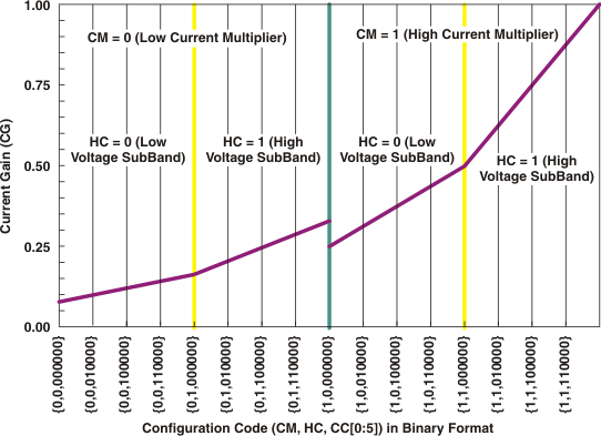 Figure 8. Current Gain vs Configuration Code
9.5.10 Error Flags Registers (EFLAG1, EFLAG2)
Table 13 describes Error Flags Registers 1 and 2.
Table 13. EFLAG1, EFLAG2 – Error Flags Registers (Address 1Dh and 1Eh) Bit Description
| ADDRESS | REGISTER | BIT | SYMBOL | ACCESS(1) | VALUE(2) | DESCRIPTION(3) |
|---|---|---|---|---|---|---|
| 1Dh | EFLAG1 | 0 | EFLAG1[0] | R | 0 | A 1 indicates an error - Channel 0 |
| 1 | EFLAG1[1] | 0 | A 1 indicates an error - Channel 1 | |||
| 2 | EFLAG1[2] | 0 | A 1 indicates an error - Channel 2 | |||
| 3 | EFLAG1[3] | 0 | A 1 indicates an error - Channel 3 | |||
| 4 | EFLAG1[4] | 0 | A 1 indicates an error - Channel 4 | |||
| 5 | EFLAG1[5] | 0 | A 1 indicates an error - Channel 5 | |||
| 6 | EFLAG1[6] | 0 | A 1 indicates an error - Channel 6 | |||
| 7 | EFLAG1[7] | 0 | A 1 indicates an error - Channel 7 | |||
| 1Eh | EFLAG2 | 0 | EFLAG1[0] | R | 0 | A 1 indicates an error - Channel 8 |
| 1 | EFLAG1[1] | 0 | A 1 indicates an error - Channel 9 | |||
| 2 | EFLAG1[2] | 0 | A 1 indicates an error - Channel 10 | |||
| 3 | EFLAG1[3] | 0 | A 1 indicates an error - Channel 11 | |||
| 4 | EFLAG1[4] | 0 | A 1 indicates an error - Channel 12 | |||
| 5 | EFLAG1[5] | 0 | A 1 indicates an error - Channel 13 | |||
| 6 | EFLAG1[6] | 0 | A 1 indicates an error - Channel 14 | |||
| 7 | EFLAG1[7] | 0 | A 1 indicates an error - Channel 15 |
9.5.11 Control Register
Following the successful acknowledgment of the slave address, LED All Call address or LED Sub Call address, the bus master sends a byte to the TLC59116, which is stored in the Control register. The lowest five bits are used as a pointer to determine which register is accessed (D[4:0]). The highest three bits are used as auto-increment flag and auto-increment options (AI[2:0]).
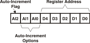 Figure 9. Control Register
When the auto-increment flag is set (AI2 = logic 1), the five low order bits of the Control register are automatically incremented after a read or write. This allows the user to program the registers sequentially. Four different types of auto-increment are possible, depending on AI1 and AI0 values.
Table 14. Auto-Increment Options
| AI2 | AI1 | AI0 | DESCRIPTION |
|---|---|---|---|
| 0 | 0 | 0 | No auto-increment |
| 1 | 0 | 0 | Auto-increment for all registers. D[4:0] roll over to 0 0000 after the last register (1 1011) is accessed. |
| 1 | 0 | 1 | Auto-increment for individual brightness registers only. D[4:0] roll over to 0 0010 after the last register (1 0001) is accessed. |
| 1 | 1 | 0 | Auto-increment for global control registers only. D[4:0] roll over to 1 0010 after the last register (1 0011) is accessed. |
| 1 | 1 | 1 | Auto-increment for individual and global control registers only. D[4:0] roll over to 0 0010 after the last register (1 0011) is accessed. |
NOTE
Other combinations are not shown in Table 14. (AI[2:0] = 001, 010, and 011) are reserved and must not be used for proper device operation.
AI[2:0] = 000 is used when the same register must be accessed several times during a single I2C bus communication, for example, changing the brightness of a single LED. Data is overwritten each time the register is accessed during a write operation.
AI[2:0] = 100 is used when all the registers must be sequentially accessed, for example, power-up programming.
AI[2:0] = 101 is used when the four LED drivers must be individually programmed with different values during the same I2C bus communication, for example, changing a color setting to another color setting.
AI[2:0] = 110 is used when the LED drivers must be globally programmed with different settings during the same I2C bus communication, for example, global brightness or blinking change.
AI[2:0] = 111 is used when individually and global changes must be performed during the same I2C bus communication, for example, changing color and global brightness at the same time.
Only the five least significant bits D[4:0] are affected by the AI[2:0] bits.
When the Control register is written, the register entry point determined by D[4:0] is the first register that will be addressed (read or write operation), and can be anywhere between 0 0000 and 1 1011 (as defined in Table 3). When AI[2] = 1, the Auto-Increment flag is set and the rollover value at which the point where the register increment stops and goes to the next one is determined by AI[2:0]. See Table 14 for rollover values. For example, if the Control register = 1111 0100 (F4h), then the register addressing sequence will be (in hex):
14 → ... → 1B → 00 → ... → 13 → 02 → ... → 13 → 02 → ... as long as the master keeps sending or reading data.