SLDS157E February 2008 – December 2014 TLC59116
PRODUCTION DATA.
- 1 Features
- 2 Applications
- 3 Description
- 4 Revision History
- 5 Description (continued)
- 6 Pin Configuration and Functions
- 7 Specifications
- 8 Parameter Measurement Information
-
9 Detailed Description
- 9.1 Overview
- 9.2 Functional Block Diagram
- 9.3 Feature Description
- 9.4 Device Functional Modes
- 9.5
Register Maps
- 9.5.1 Mode Register 1 (MODE1)"SLEEP" to "OSC" in Mode Register 1 (MODE1) Table.
- 9.5.2 Mode Register 2 (MODE2)
- 9.5.3 Brightness Control Registers 0 to 15 (PWM0 to PWM15)
- 9.5.4 Group Duty Cycle Control Register (GRPPWM)
- 9.5.5 Group Frequency Register (GRPFREQ)
- 9.5.6 LED Driver Output State Registers 0 to 3 (LEDOUT0 to LEDOUT3)
- 9.5.7 I2C Bus Subaddress Registers 1 to 3 (SUBADR1 to SUBADR3)
- 9.5.8 LED All Call I2C Bus Address Register (ALLCALLADR)
- 9.5.9 Output Gain Control Register (IREF)
- 9.5.10 Error Flags Registers (EFLAG1, EFLAG2)
- 9.5.11 Control Register
-
10Application and Implementation
- 10.1 Application Information
- 10.2 Typical Application
- 11Power Supply Recommendations
- 12Layout
- 13Device and Documentation Support
- 14Mechanical, Packaging, and Orderable Information
Package Options
Mechanical Data (Package|Pins)
Thermal pad, mechanical data (Package|Pins)
- RHB|32
Orderable Information
10 Application and Implementation
NOTE
Information in the following applications sections is not part of the TI component specification, and TI does not warrant its accuracy or completeness. TI’s customers are responsible for determining suitability of components for their purposes. Customers should validate and test their design implementation to confirm system functionality.
10.1 Application Information
10.1.1 Device Address
Following a Start condition, the bus master must output the address of the slave it is accessing.
10.1.2 Regular I2C Bus Slave Address
The I2C bus slave address of the TLC59116 is shown in Figure 10. To conserve power, no internal pullup resistors are incorporated on the hardware-selectable address pins, and they must be pulled high or low. For buffer management purposes, a set of sector information data should be stored.
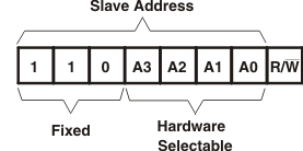 Figure 10. Slave Address
The last bit of the address byte defines the operation to be performed. When set to logic 1, a read operation is selected. When set to logic 0, a write operation is selected.
10.1.3 LED All Call I2C Bus Address
- Default power-up value (ALLCALLADR register): D0h or 1101 000
- Programmable through I2C bus (volatile programming)
- At power-up, LED All Call I2C bus address is enabled. TLC59116 sends an ACK when D0h (R/W = 0) or D1h (R/W = 1) is sent by the master.
See LED All Call I2C Bus Address Register (ALLCALLADR) for more detail.
NOTE
The default LED All Call I2C bus address (D0h or 1101 000) must not be used as a regular I2C bus slave address, since this address is enabled at power-up. All the TLC59116 devices on the I2C bus will acknowledge the address if it is sent by the I2C bus master.
10.1.4 LED Sub Call I2C Bus Address
- Three different I2C bus addresses can be used
- Default power-up values:
- SUBADR1 register: D2h or 1101 001
- SUBADR2 register: D4h or 1101 010
- SUBADR3 register: D8h or 1101 100
- Programmable through I2C bus (volatile programming)
- At power-up, Sub Call I2C bus address is disabled. TLC59116 does not send an ACK when D2h (R/W = 0) or D3h (R/W = 1) or D4h (R/W = 0) or D5h (R/W = 1) or D8h (R/W = 0) or D9h (R/W = 1) is sent by the master.
See I2C Bus Subaddress Registers 1 to 3 (SUBADR1 to SUBADR3) for more detail.
NOTE
The LED Sub Call I2C bus addresses may be used as regular I2C bus slave addresses if their corresponding enable bits are set to 0 in the MODE1 Register.
10.1.5 Software Reset I2C Bus Address
The address shown in Figure 11 is used when a reset of the TLC59116 is performed by the master. The software reset address (SWRST Call) must be used with R/W = 0. If R/W = 1, the TLC59116 does not acknowledge the SWRST. See Software Reset for more detail.
 Figure 11. Software Reset Address
NOTE
The Software Reset I2C bus address is reserved address and cannot be use as regular I2C bus slave address or as an LED All Call or LED Sub Call address.
10.1.6 Characteristics of the I2C Bus
The I2C bus is for two-way two-line communication between different devices or modules. The two lines are a serial data line (SDA) and a serial clock line (SCL). Both lines must be connected to a positive supply via a pullup resistor when connected to the output stages of a device. Data transfer may be initiated only when the bus is not busy.
10.1.6.1 Bit Transfer
One data bit is transferred during each clock pulse. The data on the SDA line must remain stable during the high period of the clock pulse as changes in the data line at this time will be interpreted as control signals (see Figure 12).
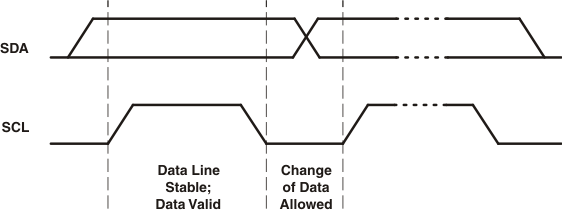 Figure 12. Bit Transfer
10.1.6.2 Start and Stop Conditions
Both data and clock lines remain high when the bus is not busy. A high-to-low transition of the data line while the clock is high is defined as the Start condition (S). A low-to-high transition of the data line while the clock is high is defined as the Stop condition (P) (see Figure 13).
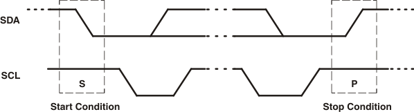 Figure 13. Start and Stop Conditions
10.1.6.3 Acknowledge
The number of data bytes transferred between the Start and the Stop conditions from transmitter to receiver is not limited. Each byte of eight bits is followed by one acknowledge bit. The acknowledge bit is a high level put on the bus by the transmitter, whereas the master generates an extra acknowledge related clock pulse.
A slave receiver that is addressed must generate an acknowledge after the reception of each byte. Also a master must generate an acknowledge after the reception of each byte that has been clocked out of the slave transmitter. The device that acknowledges has to pull down the SDA line during the acknowledge clock pulse, so that the SDA line is stable low during the high period of the acknowledge related clock pulse; set-up time and hold time must be taken into account.
A master receiver must signal an end of data to the transmitter by not generating an acknowledge on the last byte that has been clocked out of the slave. In this event, the transmitter must leave the data line high to enable the master to generate a Stop condition.
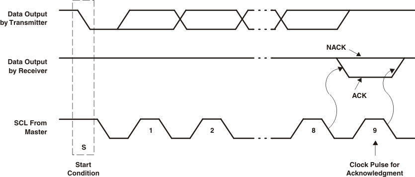 Figure 14. Acknowledge/Not Acknowledge on I2C Bus
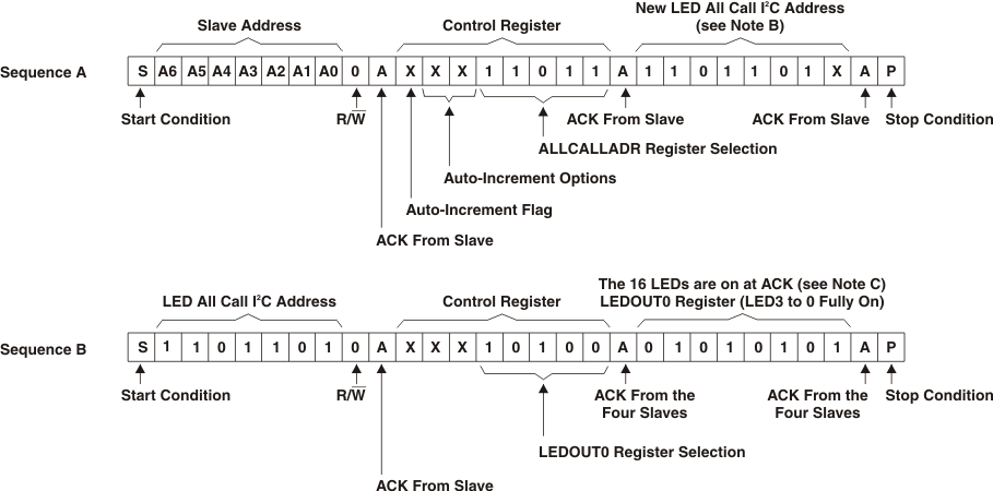
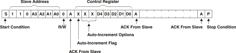 Figure 15. Write to a Specific Register
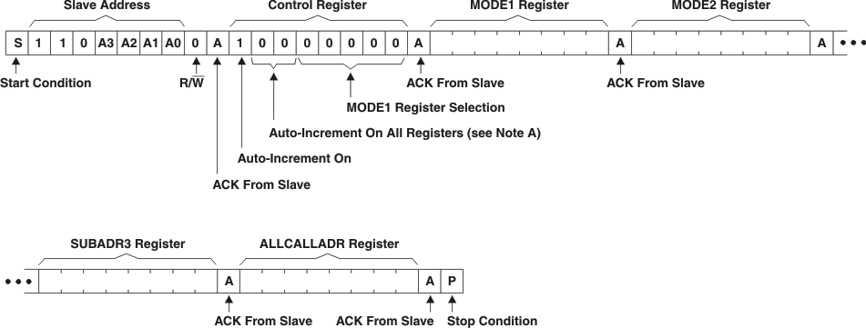
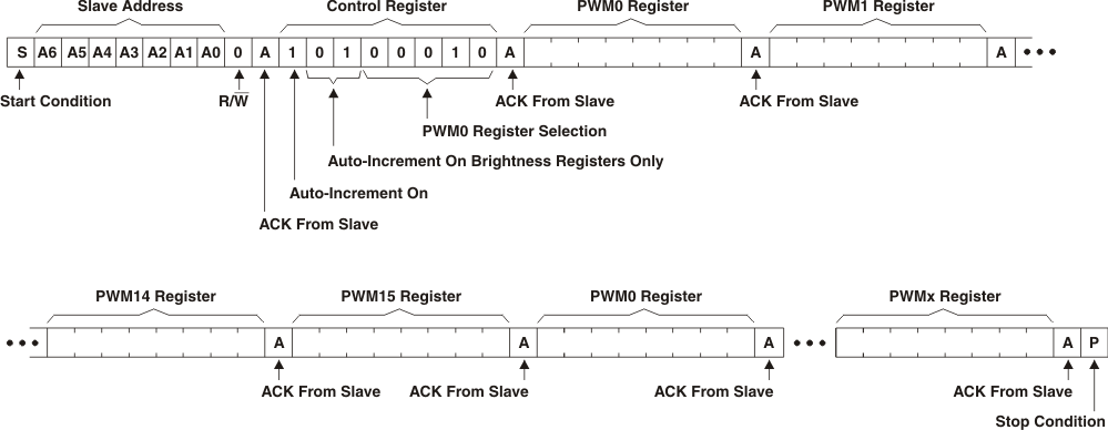 Figure 17. Multiple Writes to Individual Brightness Registers Using Auto-Increment
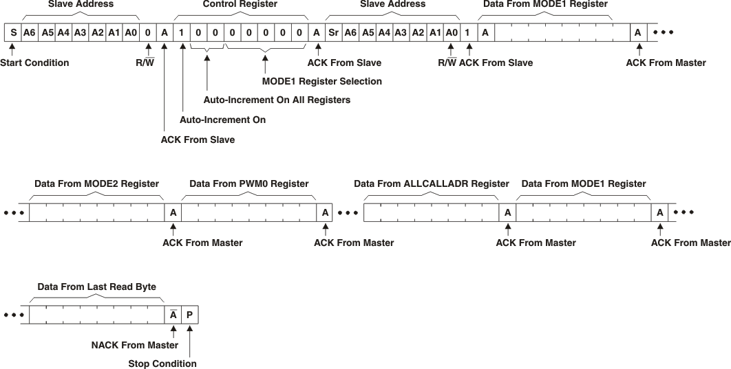 Figure 18. Read All Registers Auto-Increment
10.1.7 System Configuration
A device generating a message is a transmitter; a device receiving is the receiver. The device that controls the message is the master and the devices that are controlled by the master are the slaves (see Figure 20).
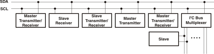 Figure 20. System Configuration
10.1.8 Constant Current Output
In LED display applications, TLC59116 provides nearly no current variations from channel to channel and from device to device. While IOUT ≤ 52 mA, the maximum current skew between channels is less than ±6% and less than ±8% between devices.
10.2 Typical Application
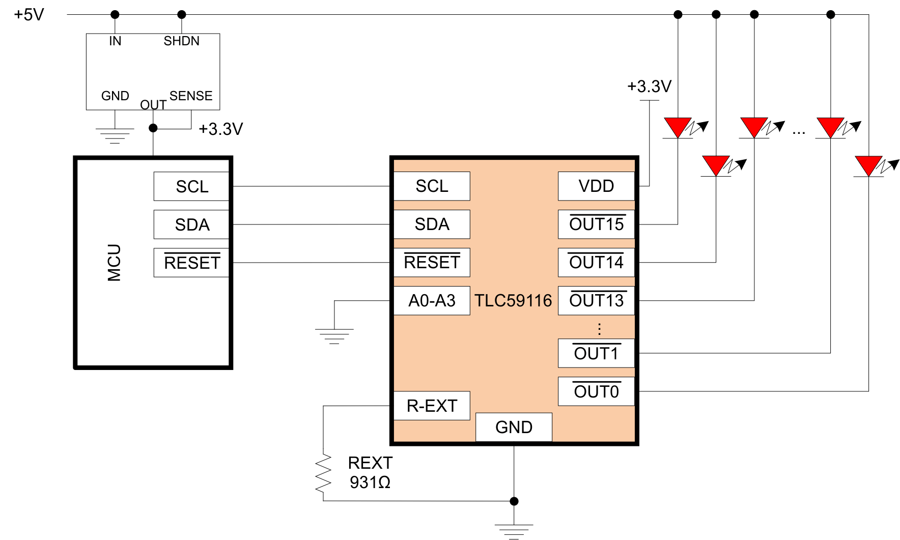 Figure 21. TLC59116 Typical Application
10.2.1 Design Requirements
Set the LED current to 20mA using the REXT resistor.
10.2.2 Detailed Design Procedure
10.2.2.1 Adjusting Output Current
TLC59116 scales up the reference current (Iref) set by the external resistor (Rext) to sink the output current (Iout) at each output port. Table 12 shows the Configuration Code and discusses bits CM, HC, and CC[5:0]. The following formulas can be used to calculate the target output current IOUT,target in the saturation region:
Where Rext is the resistance of the external resistor connected to the REXT terminal, and VREXT is the voltage of REXT, which is controlled by the programmable voltage gain (VG), which is defined by the Configuration Code.
The Current Multiplier bit (CM) sets the ratio IOUT,target/Iref to 15 or 5 (sets the exponent "CM – 1" to either 0 or –1). After power-on, the default value of VG is 127/128 = 0.992, and the default value of CM is 1, so that the ratio IOUT,target/Iref = 15. Based on the default VG and CM:
Therefore, the default current is approximately 20mA at 931 ohms.. The default relationship after power-on between IOUT,target and Rext is shown in Figure 1.
Figure 2 shows the output voltage versus the output current with several different resistor values on REXT. This shows the minimum voltage required at the device to have full VF across the LED. The VLED voltage must be higher than the VF plus the VOL of the driver. If the VLED is too high, more power will be dissipated in the driver. If this is the case, a resistor can be inserted in series with the LED to dissipate the excess power and reduce the thermal conditions on the driver.
If a single driver is used with LEDs that have different VF values, resistors can also be used in series with the LED to remove the excess power from the driver. In cases where not all outputs are being used, the unused outputs can be left floating without issue.
10.2.3 Application Curve
Figure 22 shows 20 mA of LED current along with programmed PWM dimming.
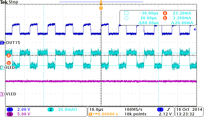 Figure 22. LED Current Set to 20 mA Through REXT