SLVS695D June 2007 – January 2015 TLC5916 , TLC5917
PRODUCTION DATA.
- 1 Features
- 2 Applications
- 3 Description
- 4 Revision History
- 5 Device Comparison Table
- 6 Pin Configuration and Functions
-
7 Specifications
- 7.1 Absolute Maximum Ratings
- 7.2 ESD Ratings
- 7.3 Recommended Operating Conditions
- 7.4 Thermal Information
- 7.5 Electrical Characteristics: VDD = 3 V
- 7.6 Electrical Characteristics: VDD = 5.5 V
- 7.7 Switching Characteristics: VDD = 3 V
- 7.8 Switching Characteristics: VDD = 5.5 V
- 7.9 Timing Requirements
- 7.10 Typical Characteristics
- 8 Parameter Measurement Information
- 9 Detailed Description
- 10Application and Implementation
- 11Power Supply Recommendations
- 12Layout
- 13Device and Documentation Support
- 14Mechanical, Packaging, and Orderable Information
Package Options
Mechanical Data (Package|Pins)
Thermal pad, mechanical data (Package|Pins)
Orderable Information
7 Specifications
7.1 Absolute Maximum Ratings
over operating free-air temperature range (unless otherwise noted)(1)| MIN | MAX | UNIT | |||
|---|---|---|---|---|---|
| VDD | Supply voltage | 0 | 7 | V | |
| VI | Input voltage | –0.4 | VDD + 0.4 | V | |
| VO | Output voltage | –0.5 | 20 | V | |
| fclk | Clock frequency | 25 | MHz | ||
| IOUT | Output current | 120 | mA | ||
| IGND | GND terminal current | 960 | mA | ||
| TA | Operating free-air temperature | –40 | 125 | °C | |
| TJ | Operating junction temperature | –40 | 150 | °C | |
| Tstg | Storage temperature | –55 | 150 | °C |
(1) Stresses beyond those listed under Absolute Maximum Ratings may cause permanent damage to the device. These are stress ratings only, which do not imply functional operation of the device at these or any other conditions beyond those indicated under Recommended Operating Conditions. Exposure to absolute-maximum-rated conditions for extended periods may affect device reliability.
7.2 ESD Ratings
| VALUE | UNIT | |||
|---|---|---|---|---|
| V(ESD) | Electrostatic discharge | Human-body model (HBM), per ANSI/ESDA/JEDEC JS-001(1) | ±1500 | V |
| Charged-device model (CDM), per JEDEC specification JESD22-C101(2) | ±500 | |||
(1) JEDEC document JEP155 states that 500-V HBM allows safe manufacturing with a standard ESD control process.
(2) JEDEC document JEP157 states that 250-V CDM allows safe manufacturing with a standard ESD control process.
7.3 Recommended Operating Conditions
| MIN | MAX | UNIT | ||||
|---|---|---|---|---|---|---|
| VDD | Supply voltage | 3 | 5.5 | V | ||
| VO | Supply voltage to output pins | OUT0–OUT7 | 20 | V | ||
| IO | Output current | DC test circuit | VO ≥ 0.6 V | 3 | mA | |
| VO ≥ 1 V | 120 | |||||
| IOH | High-level output current source | SDO shorted to GND | –1 | mA | ||
| IOL | Low-level output current sink | SDO shorted to VCC | 1 | mA | ||
| VIH | High-level input voltage | CLK, OE(ED2), LE(ED1), and SDI | 0.7 × VDD | VDD | V | |
| VIL | Low-level input voltage | CLK, OE(ED2), LE(ED1), and SDI | 0 | 0.3 × VDD | V | |
7.4 Thermal Information
| THERMAL METRIC(1) | TLC5916 | TLC5917 | UNIT | |||||
|---|---|---|---|---|---|---|---|---|
| 16 PINS | 16 PINS | |||||||
| D | N | PW | D | N | PW | |||
| RθJA | Junction-to-ambient thermal resistance | 87.4 | 51.8 | 113.9 | 87.4 | 51.8 | 114.8 | °C/W |
| RθJC(top) | Junction-to-case (top) thermal resistance | 48.1 | 39.1 | 35.2 | 48.1 | 39.1 | 35.9 | |
| RθJB | Junction-to-board thermal resistance | 44.4 | 31.8 | 59.2 | 44.4 | 31.8 | 59.8 | |
| ψJT | Junction-to-top characterization parameter | 12.5 | 23.9 | 1.3 | 12.5 | 23.9 | 1.3 | |
| ψJB | Junction-to-board characterization parameter | 44.2 | 31.7 | 58.5 | 44.2 | 31.7 | 59.2 | |
| RθJC(bot) | Junction-to-case (bottom) thermal resistance | — | — | — | — | — | — | |
(1) For more information about traditional and new thermal metrics, see the IC Package Thermal Metrics application report, SPRA953.
7.5 Electrical Characteristics: VDD = 3 V
VDD = 3 V, TJ = –40°C to 125°C (unless otherwise noted)| PARAMETER | TEST CONDITIONS | MIN | TYP(2) | MAX | UNIT | ||
|---|---|---|---|---|---|---|---|
| VDD | Input voltage | 3 | 5.5 | V | |||
| VO | Supply voltage to the output pins | 20 | V | ||||
| IO | Output current | VO ≥ 0.6 V | 3 | mA | |||
| VO ≥ 1 V | 120 | ||||||
| IOH | High-level output current, source | –1 | mA | ||||
| IOL | Low-level output current, sink | 1 | mA | ||||
| VIH | High-level input voltage | 0.7 × VDD | VDD | V | |||
| VIL | Low-level input voltage | GND | 0.3 × VDD | V | |||
| Ileak | Output leakage current | VOH = 17 V | TJ = 25°C | 0.5 | μA | ||
| TJ = 125°C | 2 | ||||||
| VOH | High-level output voltage | SDO, IOL = –1 mA | VDD – 0.4 | V | |||
| VOL | Low-level output voltage | SDO, IOH = 1 mA | 0.4 | V | |||
| IO(1) | Output current 1 | VOUT = 0.6 V, Rext = 720 Ω, CG = 0.992 | 26 | mA | |||
| Output current error, die-die | IOL = 26 mA, VO = 0.6 V, Rext = 720 Ω, TJ = 25°C | ±3% | ±6% | ||||
| Output current skew, channel-to-channel | IOL = 26 mA, VO = 0.6 V, Rext = 720 Ω, TJ = 25°C | ±1.5% | ±3% | ||||
| IO(2) | Output current 2 | VO = 0.8 V, Rext = 360 Ω, CG = 0.992 | 52 | mA | |||
| Output current error, die-die | IOL = 52 mA, VO = 0.8 V, Rext = 360 Ω, TJ = 25°C | ±2% | ±6% | ||||
| Output current skew, channel-to-channel | IOL = 52 mA, VO = 0.8 V, Rext = 360 Ω, TJ = 25°C | ±1.5% | ±3% | ||||
| IOUT vs VOUT | Output current vs output voltage regulation | VO = 1 V to 3 V, IO = 26 mA | ±0.1 | %/V | |||
| VDD = 3.0 V to 5.5 V, IO = 26 mA/120 mA | ±1 | ||||||
| Pullup resistance | OE(ED2) | 500 | kΩ | ||||
| Pulldown resistance | LE(ED1) | 500 | kΩ | ||||
| Tsd | Overtemperature shutdown(1) | 150 | 175 | 200 | °C | ||
| Thys | Restart temperature hysteresis(1) | 15 | °C | ||||
| IOUT,Th | Threshold current for open error detection | IOUT,target = 3 mA to 120 mA | 0.5 × Itarget % |
||||
| VOUT,TTh | Trigger threshold voltage for short-error detection (TLC5917 only) | IOUT,target = 3 mA to 120 mA | 2.5 | 2.7 | 3.1 | V | |
| VOUT,RTh | Return threshold voltage for short-error detection (TLC5917 only) | IOUT,target = 3 mA to 120 mA | 2.2 | V | |||
| IDD | Supply current | Rext = Open | 5 | 10 | mA | ||
| Rext = 720 Ω | 8 | 14 | |||||
| Rext = 360 Ω | 11 | 18 | |||||
| Rext = 180 Ω | 16 | 22 | |||||
(1) Specified by design.
(2) Typical values represent the likely parametric nominal values determined at the time of characterization. Typical values depend on the application and configuration and may vary over time. Typical values are not ensured on production material.
7.6 Electrical Characteristics: VDD = 5.5 V
VDD = 5.5 V, TJ = –40°C to 125°C (unless otherwise noted)| PARAMETER | TEST CONDITIONS | MIN | TYP(2) | MAX | UNIT | ||
|---|---|---|---|---|---|---|---|
| VDD | Input voltage | 3 | 5.5 | V | |||
| VO | Supply voltage to the output pins | 20 | V | ||||
| IO | Output current | VO ≥ 0.6 V | 3 | mA | |||
| VO ≥ 1 V | 120 | ||||||
| IOH | High-level output current, source | –1 | mA | ||||
| IOL | Low-level output current, sink | 1 | mA | ||||
| VIH | High-level input voltage | 0.7 × VDD | VDD | V | |||
| VIL | Low-level input voltage | GND | 0.3 × VDD | V | |||
| Ileak | Output leakage current | VOH = 17 V | TJ = 25°C | 0.5 | μA | ||
| TJ = 125°C | 2 | ||||||
| VOH | High-level output voltage | SDO, IOL = –1 mA | VDD – 0.4 | V | |||
| VOL | Low-level output voltage | SDO, IOH = 1 mA | 0.4 | V | |||
| IO(1) | Output current 1 | VOUT = 0.6 V, Rext = 720 Ω, CG = 0.992 | 26 | mA | |||
| Output current error, die-die | IOL = 26 mA, VO = 0.6 V, Rext = 720 Ω, TJ = 25°C | ±3% | ±6% | ||||
| Output current skew, channel-to-channel | IOL = 26 mA, VO = 0.6 V, Rext = 720 Ω, TJ = 25°C | ±1.5% | ±3% | ||||
| IO(2) | Output current 2 | VO = 0.8 V, Rext = 360 Ω, CG = 0.992 | 52 | mA | |||
| Output current error, die-die | IOL = 52 mA, VO = 0.8 V, Rext = 360 Ω, TJ = 25°C | ±2% | ±6% | ||||
| Output current skew, channel-to-channel | IOL = 52 mA, VO = 0.8 V, Rext = 360 Ω, TJ = 25°C | ±1.5% | ±3% | ||||
| IOUT vs VOUT | Output current vs output voltage regulation | VO = 1 V to 3 V , IO = 26 mA | ±0.1 | %/V | |||
| VDD = 3.0 V to 5.5 V, IO = 26 mA/120 mA | ±1 | ||||||
| Pullup resistance | OE(ED2), | 500 | kΩ | ||||
| Pulldown resistance | LE(ED1), | 500 | kΩ | ||||
| Tsd | Overtemperature shutdown(1) | 150 | 175 | 200 | °C | ||
| Thys | Restart temperature hysteresis(1) | 15 | °C | ||||
| IOUT,Th | Threshold current for open error detection | IOUT,target = 3 mA to 120 mA | 0.5 × Itarget% | ||||
| VOUT,TTh | Trigger threshold voltage for short-error detection (TLC5917 only) | IOUT,target = 3 mA to 120 mA | 2.5 | 2.7 | 3.1 | V | |
| VOUT,RTh | Return threshold voltage for short-error detection (TLC5917 only) | IOUT,target = 3 mA to 120 mA | 2.2 | V | |||
| IDD | Supply current | Rext = Open | 6 | 10 | mA | ||
| Rext = 720 Ω | 11 | 14 | |||||
| Rext = 360 Ω | 13 | 18 | |||||
| Rext = 180 Ω | 19 | 24 | |||||
(1) Specified by design.
(2) Typical values represent the likely parametric nominal values determined at the time of characterization. Typical values depend on the application and configuration and may vary over time. Typical values are not ensured on production material.
7.7 Switching Characteristics: VDD = 3 V
VDD = 3 V, TJ = –40°C to 125°C (unless otherwise noted)| PARAMETER | TEST CONDITIONS | MIN | TYP(2) | MAX | UNIT | |
|---|---|---|---|---|---|---|
| tPLH1 | Low-to-high propagation delay time, CLK to OUTn | VIH = VDD, VIL = GND, Rext = 360 Ω, VL = 4 V, RL = 44 Ω, CL = 10 pF, CG = 0.992 | 40 | 65 | 95 | ns |
| tPLH2 | Low-to-high propagation delay time, LE(ED1) to OUTn | 40 | 65 | 95 | ns | |
| tPLH3 | Low-to-high propagation delay time, OE(ED2) to OUTn | 40 | 65 | 95 | ns | |
| tPLH4 | Low-to-high propagation delay time, CLK to SDO | 12 | 20 | 30 | ns | |
| tPHL1 | High-to-low propagation delay time, CLK to OUTn | 300 | 365 | ns | ||
| tPHL2 | High-to-low propagation delay time, LE(ED1) to OUTn | 300 | 365 | ns | ||
| tPHL3 | High-to-low propagation delay time, OE(ED2) to OUTn | 300 | 365 | ns | ||
| tPHL4 | High-to-low propagation delay time, CLK to SDO | 12 | 20 | 30 | ns | |
| tw(CLK) | Pulse duration, CLK | 20 | ns | |||
| tw(L) | Pulse duration, LE(ED1) | 20 | ns | |||
| tw(OE) | Pulse duration, OE(ED2) | 500 | ns | |||
| tw(ED2) | Pulse duration, OE(ED2) in Error Detection Mode | 2 | μs | |||
| th(ED1,ED2) | Hold time, LE(ED1) and OE(ED2) | 10 | ns | |||
| th(D) | Hold time, SDI | 2 | ns | |||
| tsu(D,ED1) | Setup time, SDI, LE(ED1) | 3 | ns | |||
| tsu(ED2) | Setup time, OE(ED2) | 8.5 | ns | |||
| th(L) | Hold time, LE(ED1), Normal Mode | 15 | ns | |||
| tsu(L) | Setup time, LE(ED1), Normal Mode | 15 | ns | |||
| tr | Rise time, CLK(1) | 500 | ns | |||
| tf | Fall time, CLK(1) | 500 | ns | |||
| tor | Rise time, outputs (off) | 40 | 85 | 105 | ns | |
| tor | Rise time, outputs (off), TJ = 25°C | 83 | 100 | ns | ||
| tof | Rise time, outputs (on) | 100 | 280 | 370 | ns | |
| tof | Rise time, outputs (on), TJ = 25°C | 170 | 225 | ns | ||
| fCLK | Clock frequency | Cascade operation | 30 | MHz | ||
(1) If the devices are connected in cascade and tr or tf is large, it may be critical to achieve the timing required for data transfer between two cascaded devices.
(2) Typical values represent the likely parametric nominal values determined at the time of characterization. Typical values depend on the application and configuration and may vary over time. Typical values are not ensured on production material.
7.8 Switching Characteristics: VDD = 5.5 V
VDD = 5.5 V, TJ = –40°C to 125°C (unless otherwise noted)| PARAMETER | TEST CONDITIONS | MIN | TYP(2) | MAX | UNIT | |
|---|---|---|---|---|---|---|
| tPLH1 | Low-to-high propagation delay time, CLK to OUTn | VIH = VDD, VIL = GND, Rext = 360 Ω, VL = 4 V, RL = 44 Ω, CL = 10 pF, CG = 0.992 | 40 | 65 | 95 | ns |
| tPLH2 | Low-to-high propagation delay time, LE(ED1) to OUTn | 40 | 65 | 95 | ns | |
| tPLH3 | Low-to-high propagation delay time, OE(ED2) to OUTn | 40 | 65 | 95 | ns | |
| tPLH4 | Low-to-high propagation delay time, CLK to SDO | 8 | 20 | 30 | ns | |
| tPHL1 | High-to-low propagation delay time, CLK to OUTn | 300 | 365 | ns | ||
| tPHL2 | High-to-low propagation delay time, LE(ED1) to OUTn | 300 | 365 | ns | ||
| tPHL3 | High-to-low propagation delay time, OE(ED2) to OUTn | 300 | 365 | ns | ||
| tPHL4 | High-to-low propagation delay time, CLK to SDO | 8 | 20 | 30 | ns | |
| tw(CLK) | Pulse duration, CLK | 20 | ns | |||
| tw(L) | Pulse duration, LE(ED1) | 20 | ns | |||
| tw(OE) | Pulse duration, OE(ED2) | 500 | ns | |||
| tw(ED2) | Pulse duration, OE(ED2) in Error Detection Mode | 2 | μs | |||
| th(D,ED1,ED2) | Hold time, SDI, LE(ED1), and OE(ED2) | 10 | ns | |||
| th(D) | Hold time, SDI | 2 | ns | |||
| tsu(D,ED1) | Setup time, SDI, LE(ED1) | 3 | ns | |||
| tsu(ED2) | Setup time, OE(ED2) | 8.5 | ns | |||
| th(L) | Hold time, LE(ED1), Normal Mode | 15 | ns | |||
| tsu(L) | Setup time, LE(ED1), Normal Mode | 15 | ns | |||
| tr | Rise time, CLK(1) | 500 | ns | |||
| tf | Fall time, CLK(1) | 500 | ns | |||
| tor | Rise time, outputs (off) | 40 | 85 | 105 | ns | |
| tor | Rise time, outputs (off), TJ = 25°C | 83 | 100 | ns | ||
| tof | Rise time, outputs (on) | 100 | 280 | 370 | ns | |
| tof | Rise time, outputs (on), TJ = 25°C | 170 | 225 | ns | ||
| fCLK | Clock frequency | Cascade operation | 30 | MHz | ||
(1) If the devices are connected in cascade and tr or tf is large, it may be critical to achieve the timing required for data transfer between two cascaded devices.
(2) Typical values represent the likely parametric nominal values determined at the time of characterization. Typical values depend on the application and configuration and may vary over time. Typical values are not ensured on production material.
7.9 Timing Requirements
VDD = 3 V to 5.5 V (unless otherwise noted)| MIN | MAX | UNIT | |||
|---|---|---|---|---|---|
| tw(L) | LE(ED1) pulse duration | Normal Mode | 20 | ns | |
| tw(CLK) | CLK pulse duration | Normal Mode | 20 | ns | |
| tw(OE) | OE(ED2) pulse duration | Normal Mode, IOUT < 60 mA | 500 | ns | |
| Normal Mode, IOUT > 60 mA | 700 | ||||
| tsu(D) | Setup time for SDI | Normal Mode | 3 | ns | |
| th(D) | Hold time for SDI | Normal Mode | 2 | ns | |
| tsu(L) | Setup time for LE(ED1) | Normal Mode | 15 | ns | |
| th(L) | Hold time for LE(ED1) | Normal Mode | 15 | ns | |
| tw(CLK) | CLK pulse duration | Error Detection Mode | 20 | ns | |
| tw(ED2) | OE(ED2) pulse duration | Error Detection Mode | 2000 | ns | |
| tsu(ED1) | Setup time for LE(ED1) | Error Detection Mode | 4 | ns | |
| th(ED1) | Hold time for LE(ED1) | Error Detection Mode | 10 | ns | |
| tsu(ED2) | Setup time for OE(ED2) | Error Detection Mode | 6 | ns | |
| th(ED2) | Hold time for OE(ED2) | Error Detection Mode | 10 | ns | |
| fCLK | Clock frequency | Cascade operation | 30 | MHz | |
7.10 Typical Characteristics
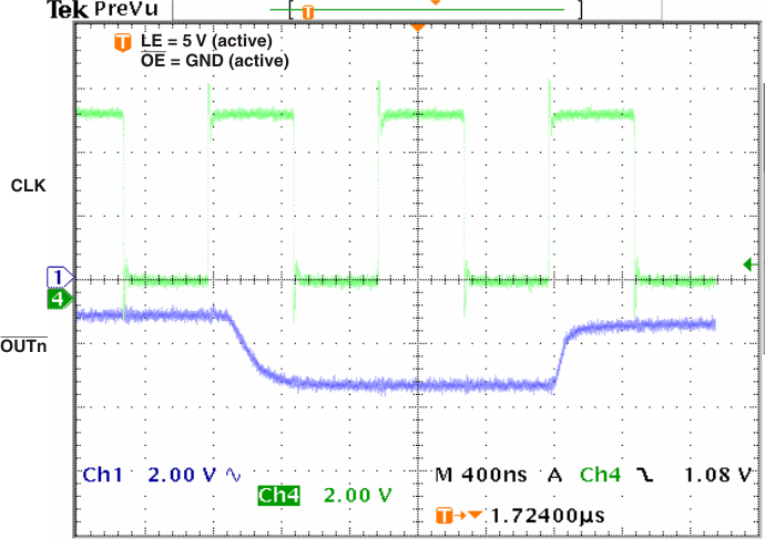 Figure 1. Response Time, CLK to OUTn
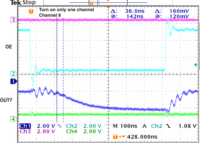 Figure 3. Response Time, OE to OUT7
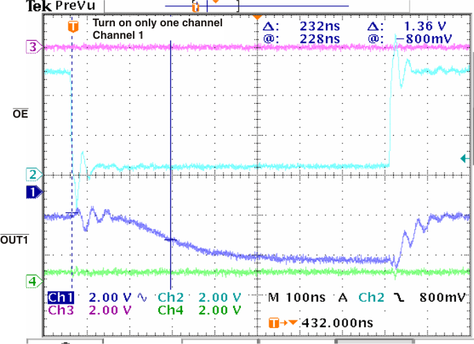 Figure 2. Response Time, OE to OUT1
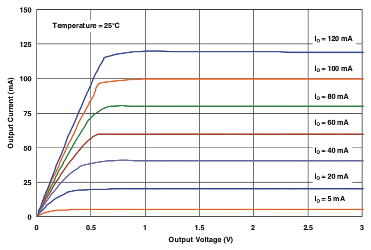 Figure 4. Output Current vs Output Voltage