SLVSCE7A May 2014 – September 2014 TLC5958
PRODUCTION DATA.
- 1 Features
- 2 Applications
- 3 Description
- 4 Typical Application Circuit (Multiple Daisy-Chained TLC5958s)
- 5 Revision History
- 6 Description (Continued)
- 7 Pin Configuration and Functions
- 8 Specifications
- 9 Parameter Measurement Information
-
10Detailed Description
- 10.1 Overview
- 10.2 Functional Block Diagram
- 10.3
Device Functional Modes
- 10.3.1 Brightness Control (BC) Function
- 10.3.2 Color Brightness Control (CC) Function
- 10.3.3 Select RIREF For a Given BC
- 10.3.4 Choosing BC/CC For a Different Application
- 10.3.5 LED Open Detection (LOD)
- 10.3.6 Power Save Mode (PSM)
- 10.3.7 Internal Pre-Charge FET
- 10.3.8 Thermal Shutdown (TSD)
- 10.3.9 IREF Resistor Short Protection (ISP)
- 10.3.10 Noise Reduction
- 11Application and Implementation
- 12Power Supply Recommendations
- 13Layout
- 14Device and Documentation Support
- 15Mechanical, Packaging, and Orderable Information
Package Options
Mechanical Data (Package|Pins)
- RTQ|56
Thermal pad, mechanical data (Package|Pins)
- RTQ|56
Orderable Information
9 Parameter Measurement Information
9.1 Pin Equivalent Input and Output Schematic Diagrams
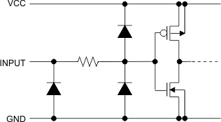 Figure 11. SIN, SCLK
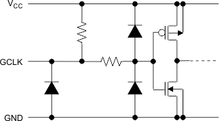 Figure 13. GCLK
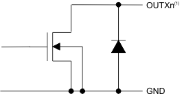
(1) X=R or G or B, n=0~15
Figure 15. OUTR0/G0/B0 Through OUTR15/G15/B15
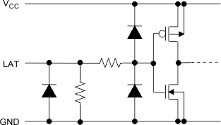 Figure 12. LAT
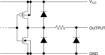 Figure 14. SOUT
9.1.1 Test Circuits
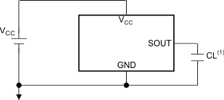
(1) CL includes measurement probe and jig capacitance.
(2) X=R or G or B, n=0~15
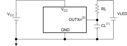
Figure 16. Rise Time and Fall Time Test Circuit for OUTXn
(1) X=R or G or B, n=0~15
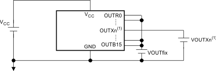
Figure 18. Constant Current Test Circuit for OUTXn
(1) CL includes measurement probe and jig capacitance.
Figure 17. Rise Time and Fall Time Test Circuit for SOUT
9.2 Timing Diagrams
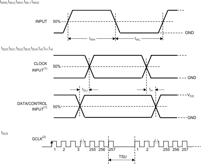
(1) Input pulse rise and fall time is 1~3ns
(2) 8 + 8 mode (SEL_PWM=0)
Figure 19. Timing Diagrams