SBVS146D August 2010 – December 2015 TLC5971
PRODUCTION DATA.
- 1 Features
- 2 Applications
- 3 Description
- 4 Revision History
- 5 Pin Configuration and Functions
- 6 Specifications
- 7 Parametric Measurement Information
-
8 Detailed Description
- 8.1 Overview
- 8.2 Functional Block Diagram
- 8.3 Feature Description
- 8.4 Device Functional Modes
- 8.5 Programming
- 9 Application and Implementation
- 10Power Supply Recommendations
- 11Layout
- 12Device and Documentation Support
- 13Mechanical, Packaging, and Orderable Information
Package Options
Mechanical Data (Package|Pins)
Thermal pad, mechanical data (Package|Pins)
Orderable Information
8 Detailed Description
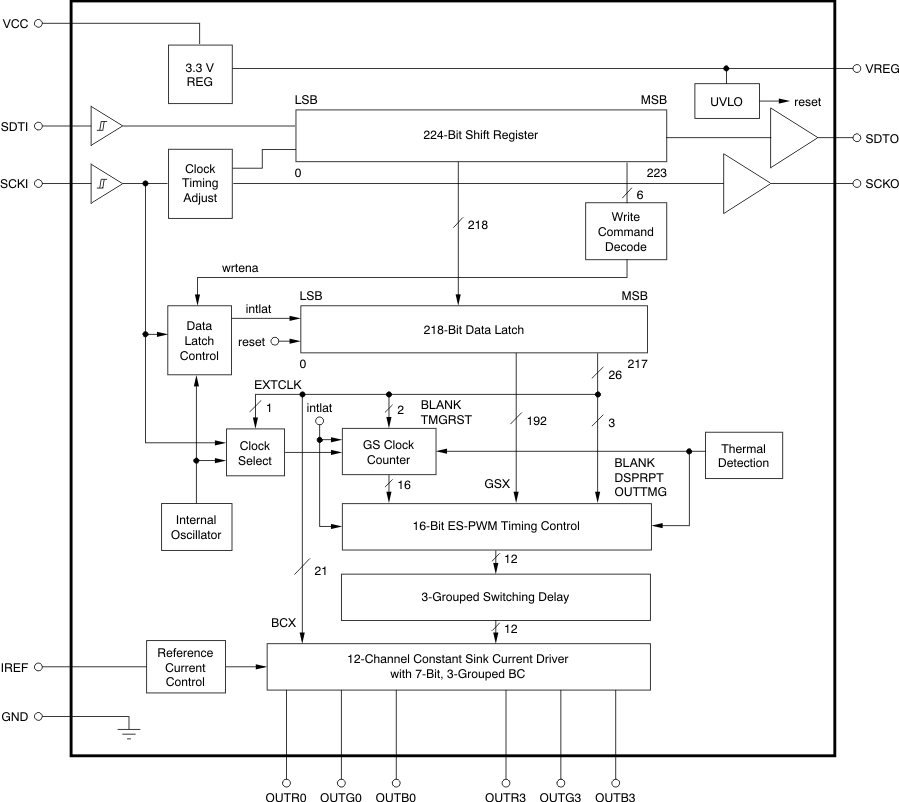
8.1 Overview
The TLC5971 is a 12-channel constant current sink driver. Each channel has an individually-adjustable, 65535-step, pulse width modulation (PWM) grayscale (GS) control. Each color has a 128-step brightness control (BC). GS data and BC data are input through a serial single-wire interface port.
The TLC5971 has a 60-mA current capability. The maximum current value of each channel is determined by the external resistor. The TLC5971 can work without external CLK signals since it can select to use internal oscillator or external GS clock.
The TLC5971 is integrated with a linear regulator that can be used for higher VCC power-supply voltage from 6 V to 17 V.
8.2 Functional Block Diagram
8.3 Feature Description
8.3.1 Auto Display Repeat Function
This function repeats the total display period without a BLANK bit change, as long as the GS reference clock is available. This function can be enabled or disabled with DSPRPT (bit 214) in the data latch. When the DSPRPT bit is 1, this function is enabled and the entire display period repeats without a BLANK bit data change. When the DSPRPT bit is 0, this function is disabled and the entire display period executes only once after the BLANK bit is set to 0 or the internal latch pulse is generated when the display timing reset function is enabled. Figure 23 shows the auto display repeat operation timing.
8.3.2 Display Timing Reset Function
This function allows the display timing to be initialized using the internal latch pulse, as shown in Figure 24. This function can be enabled or disabled by TMGRST (bit 215) in the data latch. When the TMGRST bit is 1, the GS counter is reset to 0 and all outputs are forced off when the internal latch pulse is generated. This function is the same when the BLANK bit changes (such as from 0 to 1 and from 1 to 0). Therefore, the BLANK bit does not need to be controlled from an external controller to restart the PWM control from the next GS reference clock rising edge. When this bit is 0, the GS counter is not reset and no output is forced off even if the internal latch pulse is generated. Figure 24 shows the display timing reset operation.
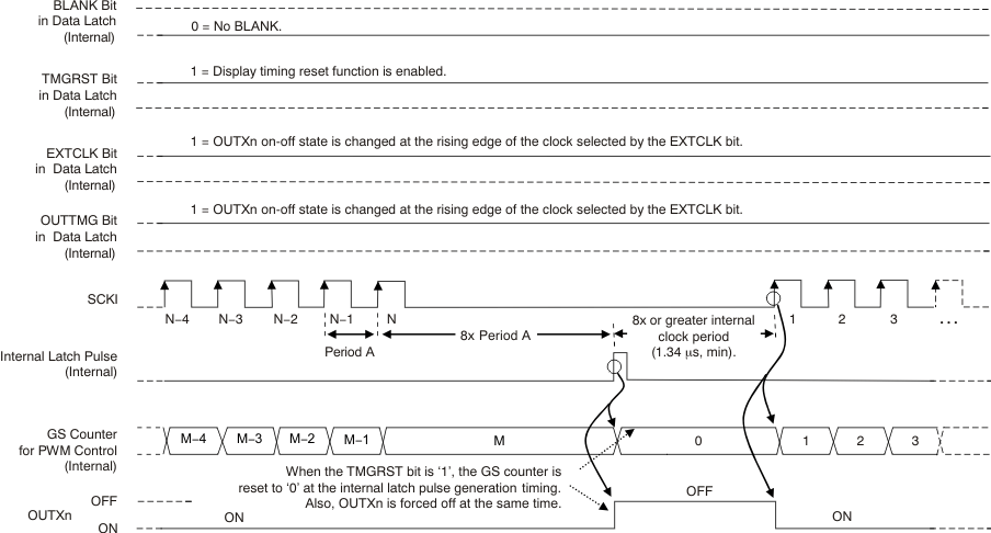 Figure 24. Display Timing Reset Function
8.3.3 Output Timing Select Function
This function selects the ON-OFF change timing of the constant-current outputs (OUTXn) set by OUTTMG (bit 217) in the data latch. When this bit is 1, OUTXn are turned on or off at the rising edge of the selected GS reference clock. When this bit is 0, OUTXn are turned on or off at the falling edge of the selected clock. Electromagnetic interference (EMI) of the total system can be reduced using this bit setting. For example, when the odd number of devices in the system have this bit set to 0 and the even number of devices in the system have this bit set to 1, EMI is reduced because the devices change the OUTXn status at a deferent timing. Figure 25 and Figure 26 show the output switching timing when the OUTTMG bit is 1 and 0, respectively.
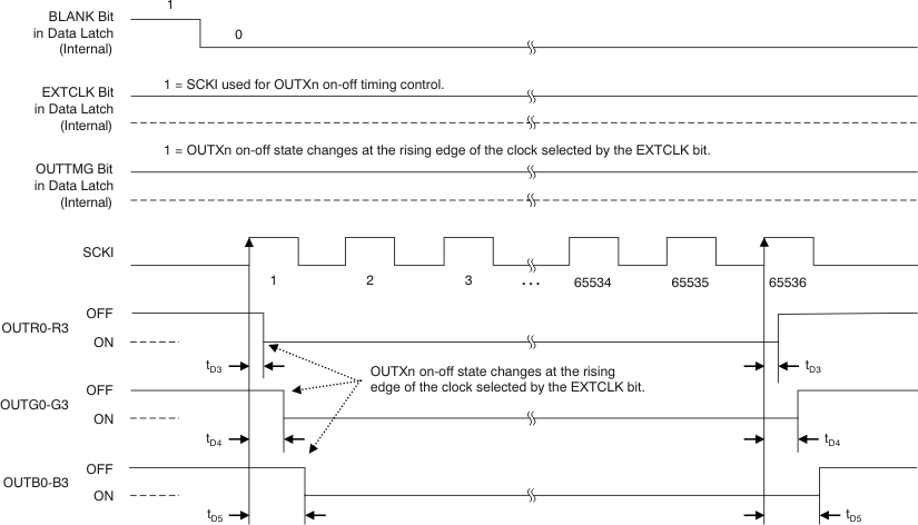 Figure 25. Output ON-OFF Timing With Four-Channel Grouped Delay (OUTTMG = 1)
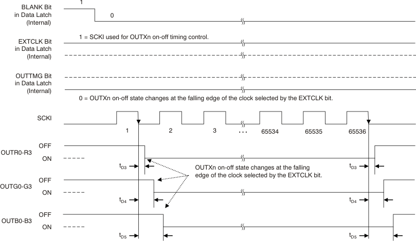 Figure 26. Output ON-OFF Timing With Four-Channel Grouped Delay (OUTTMG = 0)
8.3.4 Thermal Shutdown
The thermal shutdown (TSD) function turns off all IC constant-current outputs when the junction temperature (TJ) exceeds the threshold (TTSD = 165°C, typical). When the junction temperature drops below (TTSD – THYS), the output control starts at the first GS clock in the next display period.
8.3.5 Noise Reduction
Large surge currents may flow through the IC and the board if all 12 outputs turn on simultaneously at the start of each GS cycle. These large current surges could induce detrimental noise and EMI into other circuits. The TLC5971 turns on the outputs for each color group independently with a 25 ns (typical) rise time. The output current sinks are grouped into three groups. The first group that is turned on/off are OUTR0-3; the second group that is turned on/off are OUTG0-3; and the third group is OUTB0-3. However, the state of each output is controlled by the selected GS clock; see the Output Timing Select Function section.
8.4 Device Functional Modes
8.4.1 Maximum Constant Sink Current Setting
The maximum constant sink current value for each channel, IOLCMax, is programmed through a single resistor, RIREF, placed between IREF and GND. The desired value can be calculated with Equation 6:

where
IOLCMax is the maximum current for each output. Each output sinks the IOLCMax current when it is turned on and global brightness control data (BC) are set to the maximum value of 7Fh (127d).
RIREF must be between 0.82 kΩ and 24.8 kΩ to hold IOLCMax between 60 mA (typical) and 2 mA (typical). Otherwise, the output may be unstable. Output currents lower than 2 mA can be achieved by setting IOLCMax to 2 mA or higher and then using global brightness control to lower the output current. The constant-current sink values for specific external resistor values are shown in Figure 5 and Table 1.
Table 1. Maximum Constant-Current vs External Resistor Value
| IOLCMax (mA) | RIREF (kΩ, Typical) |
|---|---|
| 60 | 0.827 |
| 55 | 0.902 |
| 50 | 0.992 |
| 45 | 1.1 |
| 40 | 1.24 |
| 35 | 1.42 |
| 30 | 1.65 |
| 25 | 1.98 |
| 20 | 2.48 |
| 15 | 3.31 |
| 10 | 4.96 |
| 5 | 9.92 |
| 2 | 24.8 |
8.5 Programming
8.5.1 Global Brightness Control (BC) Function (Sink Current Control)
The TLC5971 has the capability to adjust all output currents of each color group (OUTR0-3, OUTG0-3, and OUTB0-3) to the same current value. This function is called global brightness (BC) control. The BC data are seven bits long, which allows each color group output current to be adjusted in 128 steps from 0% to 100% of the maximum output current, IOLCMax. The BC data are set through the serial interface. When the BC data are changed, the output current is changed immediately.
When the IC is powered on, all outputs are forced off by BLANK (bit 213). BLANK initializes in the data latch but the data in the 224-bit shift register and the 218-bit data latch are not set to a default value, except for the BLANK bit. Therefore, BC data must be written to the data latch when BLANK is set to 0.
Equation 7 determines each color group maximum output sink current:

where
Table 2 summarizes the BC data value versus the output current ratio and set current value.
Table 2. BC Data vs Current Ratio and Set Current Value
| BC DATA (BINARY) | BC DATA (DECIMAL) | BC DATA (HEX) |
OUTPUT CURRENT RATIO TO IOLCMax (%, TYPICAL) | 60 mA IOLCMax
(mA, TYPICAL) |
2 mA IOLCMax
(mA, TYPICAL) |
|---|---|---|---|---|---|
| 000 0000 | 0 | 00 | 0 | 0 | 0 |
| 000 0001 | 1 | 01 | 0.8 | 0.47 | 0.02 |
| 000 0010 | 2 | 02 | 1.6 | 0.94 | 0.03 |
| — | — | — | — | — | — |
| 111 1101 | 125 | 7D | 98.4 | 59.06 | 1.97 |
| 111 1110 | 126 | 7E | 99.2 | 59.53 | 1.98 |
| 111 1111 | 127 | 7F | 100 | 60 | 2 |
8.5.2 Grayscale (GS) Function (PWM Control)
The TLC5971 can adjust the brightness of each output channel using the enhanced spectrum pulse width modulation (ES-PWM) control scheme. The PWM bit length for each output is 16 bits. The use of the 16-bit length results in 65536 brightness steps from 0% to 100% brightness.
The PWM operation for all color groups is controlled by a 16-bit grayscale (GS) counter. The GS counter increments on each rising or falling edge of the external or internal GS reference clock that is selected by OUTTMG (bit 217) and EXTGCK (bit 216) in the data latch. When the external GS clock is selected, the GS counter uses the SCKI clock as the grayscale clock. The GS counter is reset to 0000h and all outputs are forced off when BLANK (bit 213) is set to 1 in the data latch and the counter value is held at 0 while BLANK is 1, even if the GS reference clock is toggled in between.
Equation 8 calculates each output (OUTXn) total on-time (tOUT_ON):

where
Table 3 summarizes the GS data values versus the output total ON-time and duty cycle. When the IC is powered up, BLANK (bit 213) is set to 1 to force all outputs off; however, the 224-bit shift register and the 218-bit data latch are not set to default values. Therefore, the GS data must be written to the data latch when BLANK (bit 213) is set to 0.
Table 3. Output Duty Cycle and Total On-Time versus GS Data
| GS DATA (DECIMAL) | GS DATA (HEX) | ON-TIME DUTY (%) | GS DATA (DECIMAL) | GS DATA (HEX) | ON-TIME DUTY (%) |
|---|---|---|---|---|---|
| 0 | 0 | 0 | 32768 | 8000 | 50.001 |
| 1 | 1 | 0.002 | 32769 | 8001 | 50.002 |
| 2 | 2 | 0.003 | 32770 | 8002 | 50.004 |
| 3 | 3 | 0.005 | 32771 | 8003 | 50.005 |
| — | — | — | — | — | — |
| 8191 | 1FFF | 12.499 | 40959 | 9FFF | 62.499 |
| 8192 | 2000 | 12.5 | 40960 | A000 | 62.501 |
| 8193 | 2001 | 12.502 | 40961 | A001 | 62.502 |
| — | — | — | — | — | — |
| 16383 | 3FFF | 24.999 | 49149 | BFFF | 74.997 |
| 16384 | 4000 | 25 | 49150 | C000 | 74.998 |
| 16385 | 4001 | 25.002 | 49151 | C001 | 75 |
| — | — | — | — | — | — |
| 24575 | 5FFF | 37.499 | 57343 | DFFF | 87.5 |
| 24576 | 6000 | 37.501 | 57344 | E000 | 87.501 |
| 24577 | 6001 | 37.502 | 57345 | E001 | 87.503 |
| — | — | — | — | — | — |
| 32765 | 7FFD | 49.996 | 65533 | FFFD | 99.997 |
| 32766 | 7FFE | 49.998 | 65534 | FFFE | 99.998 |
| 32767 | 7FFF | 49.999 | 65535 | FFFF | 100 |
8.5.3 Enhanced Spectrum (ES) PWM Control
Enhanced spectrum (ES) PWM has the total display period divided into 128 display segments. The total display period refers the period between the first grayscale clock input to the 65536th grayscale clock input after BLANK (bit 213) is set to 0. Each display period has 512 grayscale values, maximum. Each output on-time changes depending on the grayscale data. Refer to Table 4 for sequence information and Figure 27 for timing information.
Table 4. ES-PWM Drive Turnon Time Length
| GS DATA (DEC) | GS DATA (HEX) | OUTn DRIVER OPERATION |
|---|---|---|
| 0 | 0000h | Does not turn on |
| 1 | 0001h | Turns on during one GS clock period in the 1st display period |
| 2 | 0002h | Turns on during one GS clock period in the 1st and 65th display period |
| 3 | 0003h | Turns on during one GS clock period in the 1st, 33rd, and 65th display period |
| 4 | 0004h | Turns on during one GS clock period in the 1st, 33rd, 65th, and 97th display period |
| 5 | 0005h | Turns on during one GS clock period in the 1st, 17th, 33rd, 65th, and 97th display period |
| 6 | 0006h | Turns on during one GS clock period in the 1st, 17th, 33rd, 65th, 81st, and 97th display period |
| — | — | The number of display periods that OUTXn is turned on during one GS clock is incremented by the GS data increasing in the following order. The order of display periods that the output turns on are: 1, 65, 33, 97, 17, 81, 49, 113, 9, 73, 41, 105, 25, 89, 57, 121, 5, 69, 37, 101, 21, 85, 53, 117, 13, 77, 45, 109, 29, 93, 61, 125, 3, 67, 35, 99, 19, 83, 51, 115, 11, 75, 43, 107, 27, 91, 59, 123, 7, 71, 39, 103, 23, 87, 55, 119, 15, 79, 47, 111, 31, 95, 63, 127, 2, 66, 34, 98, 18, 82, 50, 114, 10, 74, 42, 106, 26, 90, 58, 122, 6, 70, 38, 102, 22, 86, 54, 118, 14, 78, 46, 110, 30, 94, 62, 126, 4, 68, 36, 100, 20, 84, 52, 116, 12, 76, 44, 108, 28, 92, 60, 124, 8, 72, 40, 104, 24, 88, 56, 120, 16, 80, 48, 112, 32, 96, 64, and 128. |
| 127 | 007Fh | Turns on during one GS clock period in the 1st to 127th display period, but does not turn on in the 128th display period |
| 128 | 0080h | Turns on during one GS clock period in all display periods (1st to 128th) |
| 129 | 0081h | Turns on during two GS clock periods in the 1st display period and one GS clock period in the next display period |
| — | — | The number of display periods where OUTn is turned on for two GS clocks is incremented by the increased GS data similar to the previous case where the GS value is 1 trough 127 |
| 255 | 00FFh | Turns on during two GS clock periods in the 1st to 127th display period, but only turns on during one GS clock period in the 128th display period |
| 256 | 0100h | Turns on during two GS clock periods in all display periods (1st to 128th) |
| 257 | 0101h | Turns on during three GS clock periods in the 1st display period and two GS clock periods in the next display period |
| — | — | Display periods with OUTn turned on is incremented by the increased GS datasimilar to 0101h operation |
| 65478 | FEFFh | Turns on during 511 GS clock periods in the 1st to 127th display period, but only turns on 510 GS clock periods in the 128th display period |
| 65280 | FF00h | Turns on during 511 GS clock periods in all display periods (1st to 128th) |
| 65281 | FF01h | Turns on during 512 GS clock periods in the 1st display period and 511 GS clock periods in the 2nd to 128th display periods |
| — | — | — |
| 65534 | FFFEh | Turns on during 512 GS clock periods in the 1st to 63th and 65th to 127th display periods, and turns on 511 GS clock periods in the 64th and 128th display periods |
| 65535 | FFFFh | Turns on during 512 GS clock periods in the 1st to 127th display period, but only turns on 511 GS clock periods in the 128th display period |
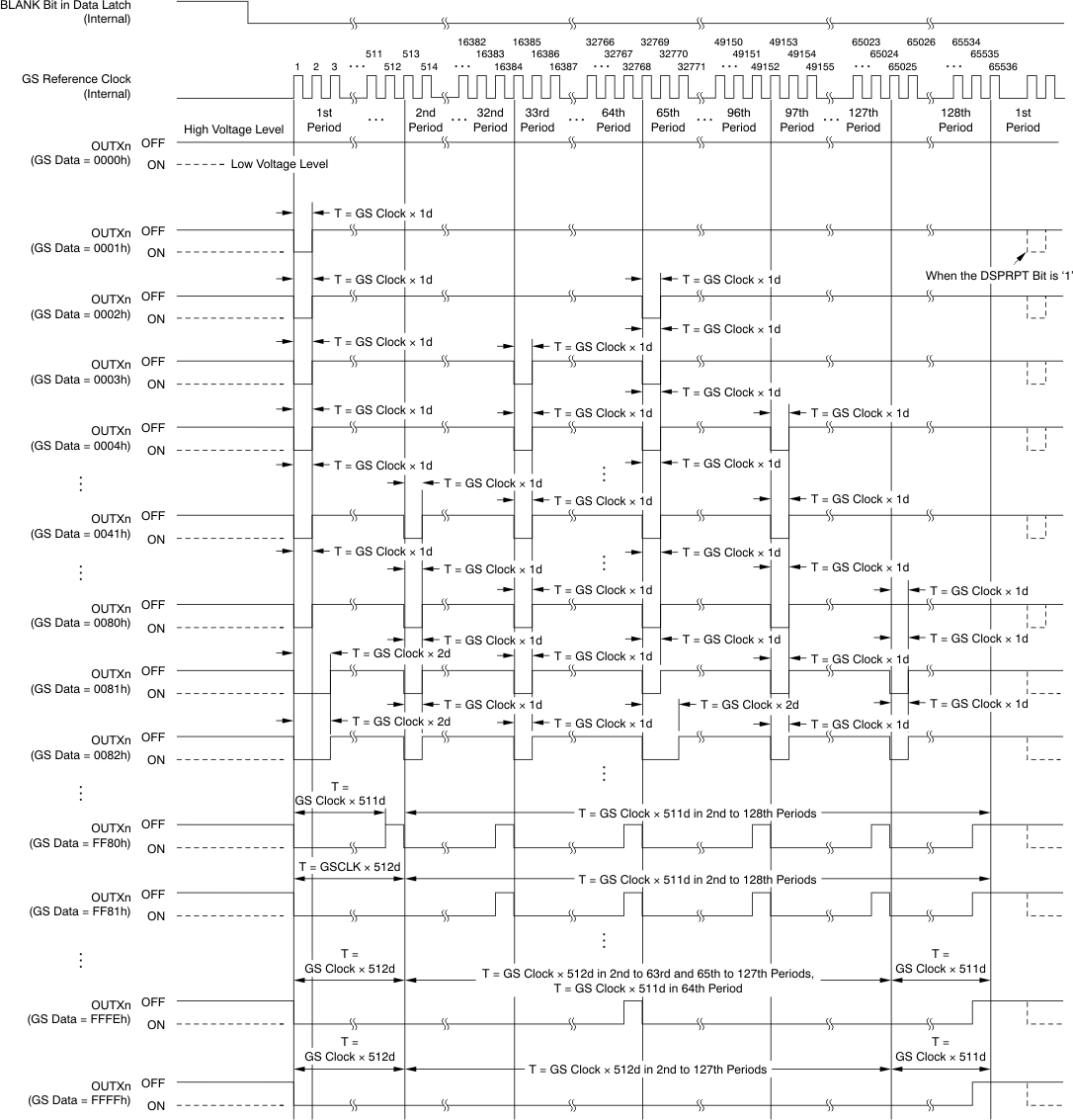 Figure 27. ES-PWM Operation
8.5.4 Register and Data Latch Configuration
The TLC5971 has a 224-bit shift register and a 218-bit data latch that set grayscale (GS) data, global brightness control (BC), and function control (FC) data into the device. When the internal latch pulse is generated and the data of the six MSBs in the shift register are 25h, the 218 following data bits in the shift register are copied into the 218-bit data latch. If the data of the six MSBs is not 25h, the 218 data bits are not copied into the 218-bit data latch. The data in the data latch are used for GS, BC, and FC functions. Figure 28 shows the shift register and the data latch configuration.
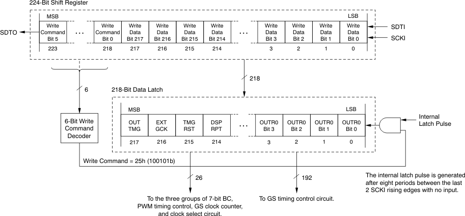 Figure 28. Common Shift Register and Control Data Latch Configuration
8.5.4.1 224-Bit Shift Register
The 224-bit shift register is used to input data from the SDTI pin with the SCKI clock into the TLC5971. The shifted data in this register is used for GS, BC, and FC. The six MSBs are used for the write command. The LSB of the register is connected to the SDTI pin and the MSB is connected to the SDTO pin. On each SCKI rising edge, the data on SDTI are shifted into the register LSB and all 224 bits are shifted towards the MSB. The register MSB is always connected to SDTO. When the device is powered up, the data in the 224-bit shift register is not set to any default value.
8.5.4.2 218-Bit Data Latch
The 218-bit data latch is used to latch the GS, BC, and FC data. The 218 LSBs in the 244-bit shift register are copied to the data latch when the internal latch pulse is generated with the 6-bit write command, 25h (100101b). When the device is powered up, the data in the latch are not reset except for BLANK (bit 213) which is set to 1 to force all outputs off. Therefore, GS, BC, and FC data must be set to the proper values before BLANK is set to 0. The 218-bit data latch configuration is shown in Figure 29 and the data bit assignment is shown in Table 5.
 Figure 29. 218-Bit Data Latch Configuration
Table 5. Data Latch Bit Assignment
8.5.5 Internal Latch Pulse Generation Timing
The internal latch pulse is generated when the SCKI rising edge does not change for 8x the period between the last SCKI rising edge and the second to last SCKI rising edge if the data of the six MSBs in the 244-bit shift register are the command code 25h. The generation timing changes as a result of the SCKI frequency with the time range between 16384 times the internal oscillator period (2.74 ms), maximum, and 8x the internal oscillator period (666 ns), minimum. Figure 30 shows the internal latch pulse generation timing.
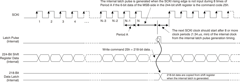 Figure 30. Data Latch Pulse Generation Timing
