SBVS222C February   2013  – October 2016 TLC59731

PRODUCTION DATA.  

  1. Features
  2. Applications
  3. Description
  4. Revision History
  5. Pin Configuration and Functions
  6. Specifications
    1. 6.1 Absolute Maximum Ratings
    2. 6.2 ESD Ratings
    3. 6.3 Recommended Operating Conditions
    4. 6.4 Thermal Information
    5. 6.5 Electrical Characteristics
    6. 6.6 Switching Characteristics
    7. 6.7 Typical Characteristics
  7. Parameter Measurement Information
    1. 7.1 Pin-Equivalent Input and Output Schematic Diagrams
    2. 7.2 Test Circuits
  8. Detailed Description
    1. 8.1 Overview
    2. 8.2 Functional Block Diagram
    3. 8.3 Feature Description
      1. 8.3.1 Sink Current Value Setting
      2. 8.3.2 Resistor and Capacitor Value Setting for Shunt Regulator
      3. 8.3.3 Grayscale (GS) Control
      4. 8.3.4 EasySet and Shunt Regulator
      5. 8.3.5 No Limit Cascading
      6. 8.3.6 Connector Design
    4. 8.4 Device Functional Modes
      1. 8.4.1 Grayscale (GS) Function (PWM Control)
        1. 8.4.1.1 PWM Control
    5. 8.5 Programming
      1. 8.5.1 One-Wire Interface (EasySet) Data Writing Method
        1. 8.5.1.1 Data Transfer Rate (TCYCLE) Measurement Sequence
        2. 8.5.1.2 Data 0 and Data 1 Write Sequence (Data Write Sequence)
        3. 8.5.1.3 One Communication Cycle End of Sequence (EOS)
        4. 8.5.1.4 GS Data Latch (GSLAT) Sequence
        5. 8.5.1.5 How to Control Devices Connected in Series
    6. 8.6 Register Maps
      1. 8.6.1 Register and Data Latch Configuration
  9. Application and Implementation
    1. 9.1 Application Information
    2. 9.2 Typical Application
      1. 9.2.1 Design Requirements
      2. 9.2.2 Detailed Design Procedure
        1. 9.2.2.1 Define Basic Parameters
        2. 9.2.2.2 Grayscale (GS) Data
      3. 9.2.3 Application Curve
    3. 9.3 System Examples
    4. 9.4 Do's and Don'ts
  10. 10Power Supply Recommendations
  11. 11Layout
    1. 11.1 Layout Guidelines
    2. 11.2 Layout Example
  12. 12Device and Documentation Support
    1. 12.1 Receiving Notification of Documentation Updates
    2. 12.2 Community Resources
    3. 12.3 Trademarks
    4. 12.4 Electrostatic Discharge Caution
    5. 12.5 Glossary
  13. 13Mechanical, Packaging, and Orderable Information

Package Options

Mechanical Data (Package|Pins)
Thermal pad, mechanical data (Package|Pins)
Orderable Information

5 Pin Configuration and Functions

D Package
8-Pin SOIC
Top View
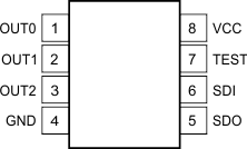
TLC59731 po_bvs222.gif

Pin Functions

PIN I/O DESCRIPTION
NAME NO.
GND 4 Power ground
OUT0 1 O Sink driver outputs.
Multiple outputs can be configured in parallel to increase the sink drive current capability.
Different voltages can be applied to each output.
OUT1 2 O
OUT2 3 O
SDI 6 I Serial data input. This pin is internally pulled down to GND with a 1-MΩ (typical) resistor.
SDO 5 O Serial data output
TEST 7 TI internal test terminal. This pin must be connected to GND or left open.
VCC 8 Power-supply voltage