SLLSFM5B March 2021 – February 2024 TLIN2029A-Q1
PRODUCTION DATA
- 1
- 1 Features
- 2 Applications
- 3 Description
- 4 Pin Configuration and Functions
- 5 Specifications
- 6 Parameter Measurement Information
-
7 Detailed Description
- 7.1 Overview
- 7.2 Functional Block Diagram
- 7.3
Feature Description
- 7.3.1 LIN (Local Interconnect Network) Bus
- 7.3.2 TXD (Transmit Input and Output)
- 7.3.3 RXD (Receive Output)
- 7.3.4 VSUP (Supply Voltage)
- 7.3.5 GND (Ground)
- 7.3.6 EN (Enable Input)
- 7.3.7 Protection Features
- 7.3.8 TXD Dominant Time Out (DTO)
- 7.3.9 Bus Stuck Dominant System Fault: False Wake Up Lockout
- 7.3.10 Thermal Shutdown
- 7.3.11 Under Voltage on VSUP
- 7.3.12 Unpowered Device and LIN Bus
- 7.4 Device Functional Modes
- 8 Application Information Disclaimer
- 9 Device and Documentation Support
- 10Revision History
- 11Mechanical, Packaging, and Orderable Information
Package Options
Mechanical Data (Package|Pins)
Thermal pad, mechanical data (Package|Pins)
- DRB|8
Orderable Information
8.2 Typical Application
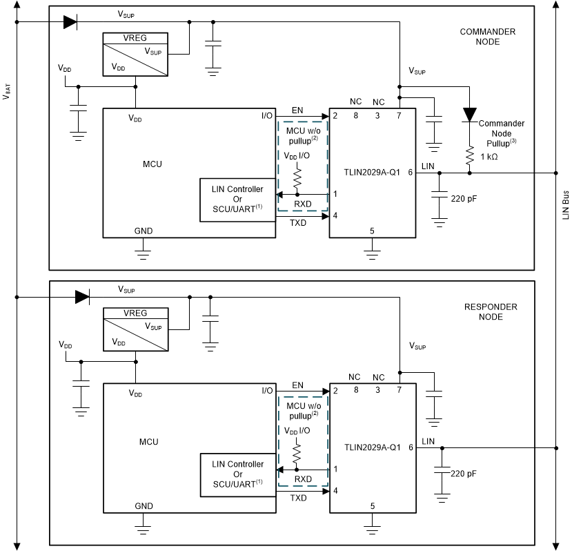
The device integrates a 45kΩ pull-up resistor and series diode for responder node applications. For commander applications, an external 1kΩ pull-up resistor with series blocking diode can be used. Figure 8-1 shows the device being used in both commander mode and responder mode applications.

A. If RXD on MCU on LIN responder node has
internal pullup; no external pullup resistor is needed.
B. If RXD on MCU or LIN responder node does
not have an internal pullup requires external pullup resistor.
C. Commander node applications require and
external 1 kΩ pullup resistor and serial diode.
D. Decoupling capacitor values on
VSUP are system dependent but usually have 100nF, 1µF and ≥ 10µF.
Figure 8-1 Typical LIN
Bus