SLOSE29A November 2018 – November 2022 TLV1704-SEP
PRODUCTION DATA
- 1 Features
- 2 Applications
- 3 Description
- 4 Revision History
- 5 Pin Configuration and Functions
- 6 Specifications
- 7 Detailed Description
- 8 Application and Implementation
- 9 Device and Documentation Support
- 10Mechanical, Packaging, and Orderable Information
Package Options
Mechanical Data (Package|Pins)
- PW|14
Thermal pad, mechanical data (Package|Pins)
- PW|14
Orderable Information
7.3.1 Comparator Inputs
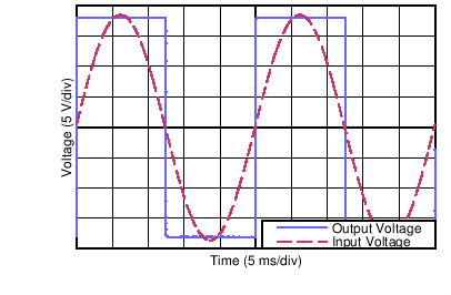
The TLV1704-SEP device is a rail-to-rail input comparator, with an input common-mode range that includes the supply rails. The TLV1704-SEP device is designed to prevent phase inversion when the input pins exceed the supply voltage. Figure 7-1 shows the TLV1704-SEP device response when input voltages exceed the supply, resulting in no phase inversion.
 Figure 7-1 No Phase Inversion: Comparator Response to Input Voltage (Propagation Delay Included)