SLOS270F March 2001 – August 2016 TLV2370 , TLV2371 , TLV2372 , TLV2373 , TLV2374 , TLV2375
PRODUCTION DATA.
- 1 Features
- 2 Applications
- 3 Description
- 4 Revision History
- 5 Device Comparison Tables
- 6 Pin Configuration and Functions
-
7 Specifications
- 7.1 Absolute Maximum Ratings
- 7.2 Recommended Operating Conditions
- 7.3 Thermal Information: TLV2370
- 7.4 Thermal Information: TLV2371
- 7.5 Thermal Information: TLV2372
- 7.6 Thermal Information: TLV2373
- 7.7 Thermal Information: TLV2374
- 7.8 Thermal Information: TLV2375
- 7.9 Electrical Characteristics
- 7.10 Typical Characteristics
- 8 Detailed Description
- 9 Application and Implementation
- 10Power Supply Recommendations
- 11Layout
- 12Device and Documentation Support
- 13Mechanical, Packaging, and Orderable Information
Package Options
Mechanical Data (Package|Pins)
Thermal pad, mechanical data (Package|Pins)
Orderable Information
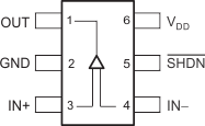
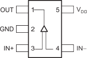
6 Pin Configuration and Functions
TLV2370 DBV Package
6-Pin SOT-23
Top View
TLV2370 D and P Packages
8-Pin SOIC and PDIP
Top View
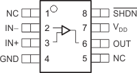
Pin Functions: TLV2370
| PIN | I/O | DESCRIPTION | ||
|---|---|---|---|---|
| NAME | SOT-23 | SOIC, PDIP | ||
| GND | 2 | 4 | — | Ground connection |
| IN– | 4 | 2 | I | Negative (inverting) input |
| IN+ | 3 | 3 | I | Positive (noninverting) input |
| NC | — | 1, 5 | — | No internal connection (can be left floating) |
| OUT | 1 | 6 | O | Output |
| SHDN | 5 | 8 | I | Shutdown control (active low, can be left floating) |
| VDD | 6 | 7 | — | Positive power supply |
TLV2371 DBV Package
5-Pin SOT-23
Top View
TLV2371 D and P Packages
8-Pin SOIC and PDIP
Top View
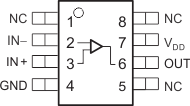
Pin Functions: TLV2371
| PIN | I/O | DESCRIPTION | ||
|---|---|---|---|---|
| NAME | SOT-23 | SOIC, PDIP | ||
| GND | 2 | 4 | — | Ground connection |
| IN– | 4 | 2 | I | Negative (inverting) input |
| IN+ | 3 | 3 | I | Positive (noninverting) input |
| NC | — | 1, 5, 8 | — | No internal connection (can be left floating) |
| OUT | 1 | 6 | O | Output |
| VDD | 5 | 7 | — | Positive power supply |
TLV2372 D, DGK, and P Packages
8-Pin SOIC, VSSOP, and PDIP
Top View

Pin Functions: TLV2372
TLV2373 DGS Package
10-Pin VSSOP
Top View
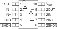
TLV2373 D and N Packages
14-Pin SOIC and PDIP
Top View
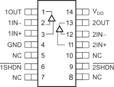
Pin Functions: TLV2373
| PIN | I/O | DESCRIPTION | ||
|---|---|---|---|---|
| NAME | SOIC, PDIP | VSSOP | ||
| GND | 4 | 4 | — | Ground connection |
| 1IN– | 2 | 2 | I | Inverting input, channel 1 |
| 1IN+ | 3 | 3 | I | Noninverting input, channel 1 |
| 2IN– | 12 | 8 | I | Inverting input, channel 2 |
| 2IN+ | 11 | 7 | I | Noninverting input, channel 2 |
| 1OUT | 1 | 1 | O | Output, channel 1 |
| 2OUT | 13 | 9 | O | Output, channel 2 |
| 1SHDN | 6 | 5 | I | Shutdown control, channel 1, (active low, can be left floating) |
| 2SHDN | 9 | 6 | I | Shutdown control, channel 2, (active low, can be left floating) |
| VDD | 14 | 10 | — | Positive power supply |
| NC | 5, 7, 8, 10 | — | — | No internal connection (can be left floating) |
TLV2374 D, N, and PW Packages
14-Pin SOIC, PDIP, and TSSOP
Top View
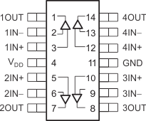
Pin Functions: TLV2374
| PIN | I/O | DESCRIPTION | |
|---|---|---|---|
| NAME | SOIC, PDIP, TSSOP | ||
| GND | 11 | — | Ground connection |
| 1IN– | 2 | I | Inverting input, channel 1 |
| 1IN+ | 3 | I | Noninverting input, channel 1 |
| 2IN– | 6 | I | Inverting input, channel 2 |
| 2IN+ | 5 | I | Noninverting input, channel 2 |
| 3IN– | 9 | I | Inverting input, channel 3 |
| 3IN+ | 10 | I | Noninverting input, channel 3 |
| 4IN– | 13 | I | Inverting input, channel 4 |
| 4IN+ | 12 | I | Noninverting input, channel 4 |
| 1OUT | 1 | O | Output, channel 1 |
| 2OUT | 7 | O | Output, channel 2 |
| 3OUT | 8 | O | Output, channel 3 |
| 4OUT | 14 | O | Output, channel 4 |
| VDD | 4 | — | Positive power supply |
TLV2375 D, N, and PW Packages
16-Pin SOIC, PDIP, and TSSOP
Top View
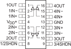
Pin Functions: TLV2375
| PIN | I/O | DESCRIPTION | |
|---|---|---|---|
| NAME | SOIC, PDIP, TSSOP | ||
| GND | 13 | — | Ground connection |
| 1IN– | 2 | I | Inverting input, channel 1 |
| 2IN– | 6 | I | Inverting input, channel 2 |
| 3IN– | 11 | I | Inverting input, channel 3 |
| 4IN– | 15 | I | Inverting input, channel 4 |
| 1IN+ | 3 | I | Noninverting input, channel 1 |
| 2IN+ | 5 | I | Noninverting input, channel 2 |
| 3IN+ | 12 | I | Noninverting input, channel 3 |
| 4IN+ | 14 | I | Noninverting input, channel 4 |
| 1OUT | 1 | O | Output, channel 1 |
| 2OUT | 7 | O | Output, channel 2 |
| 3OUT | 10 | O | Output, channel 3 |
| 4OUT | 16 | O | Output, channel 4 |
| 1/2SHDN | 8 | I | Shutdown control, channels 1 and 2, (active low, can be left floating) |
| 3/4SHDN | 9 | I | Shutdown control, channels 3 and 4, (active low, can be left floating) |
| VDD | 4 | — | Positive power supply |
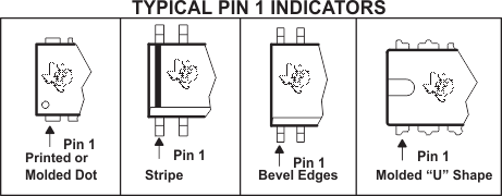
If there is not a Pin 1 indicator, turn device to enable reading the symbol from the left to right. Pin 1 is at the lower left corner of the device.
Figure 1. Typical Pin 1 Indicators