SLAS784A March 2012 – September 2015 TLV320AIC3212
PRODUCTION DATA.
- 1 Features
- 2 Applications
- 3 Description
- 4 Revision History
- 5 Description (continued)
- 6 Device Comparison Table
- 7 Pin Configuration and Functions
-
8 Specifications
- 8.1 Absolute Maximum Ratings
- 8.2 ESD Ratings
- 8.3 Recommended Operating Conditions
- 8.4 Thermal Information
- 8.5 Electrical Characteristics, SAR ADC
- 8.6 Electrical Characteristics, ADC
- 8.7 Electrical Characteristics, Bypass Outputs
- 8.8 Electrical Characteristics, Microphone Interface
- 8.9 Electrical Characteristics, Audio DAC Outputs
- 8.10 Electrical Characteristics, Class-D Outputs
- 8.11 Electrical Characteristics, Miscellaneous
- 8.12 Electrical Characteristics, Logic Levels
- 8.13 Audio Data Serial Interface Timing (I2S): I2S/LJF/RJF Timing in Master Mode
- 8.14 Audio Data Serial Interface Timing (I2S): I2S/LJF/RJF Timing in Slave Mode
- 8.15 Typical DSP Timing: DSP/Mono PCM Timing in Master Mode
- 8.16 Typical DSP Timing: DSP/Mono PCM Timing in Slave Mode
- 8.17 I2C Interface Timing
- 8.18 SPI Timing
- 8.19 Typical Characteristics
- 9 Parameter Measurement Information
-
10Detailed Description
- 10.1 Overview
- 10.2 Functional Block Diagram
- 10.3
Feature Description
- 10.3.1 Device Connections
- 10.3.2
Analog Audio I/O
- 10.3.2.1 Analog Low Power Bypass
- 10.3.2.2
Headphone Outputs
- 10.3.2.2.1 Using the Headphone Amplifier
- 10.3.2.2.2 Ground-Centered Headphone Amplifier Configuration
- 10.3.2.2.3 Stereo Unipolar Configuration
- 10.3.2.2.4 Mono Differential DAC to Mono Differential Headphone Output
- 10.3.2.3 Stereo Line Outputs
- 10.3.2.4 Differential Receiver Output
- 10.3.2.5 Stereo Class-D Speaker Outputs
- 10.3.3 ADC / Digital Microphone Interface
- 10.3.4 DAC
- 10.3.5 Device Power Consumption
- 10.3.6 Powertune
- 10.3.7 Clock Generation and PLL
- 10.3.8 Interfaces
- 10.3.9 Device Special Functions
- 10.4 Device Functional Modes
- 10.5 Register Maps
- 11Application and Implementation
- 12Power Supply Recommendations
- 13Layout
- 14Device and Documentation Support
- 15Mechanical, Packaging, and Orderable Information
Package Options
Mechanical Data (Package|Pins)
- YZF|81
Thermal pad, mechanical data (Package|Pins)
Orderable Information
13 Layout
13.1 Layout Guidelines
Each system design and PCB layout is unique. The layout should be carefully reviewed in the context of a specific PCB design. However, the following guidelines can optimize TLV320AIC3212 performance:
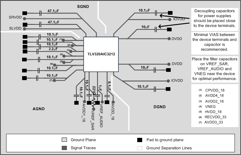
- The decoupling capacitors for the power supplies should be placed close to the device terminals. Figure 33 shows the recommended decoupling capacitors for the TLV320AIC3212.
- Place the flying capacitor between CPFCP and CPFCM near the device terminals, with minimal VIAS in the trace between the device terminals and the capacitor. Similarly, keep the decoupling capacitor on VNEG near the device terminal with minimal VIAS in the trace between the device terminal, capacitor, and PCB ground.
- TLV320AIC3212 internal voltage references must be filtered using external capacitors. Place the filter capacitors on VREF_SAR and VREF_AUDIO near the device terminals for optimal performance.
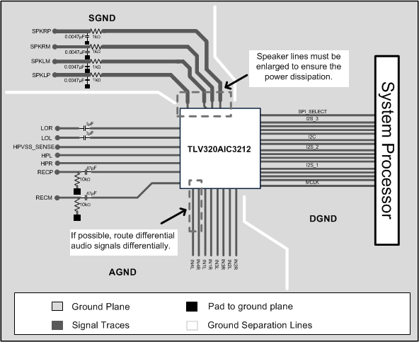
- For analog differential audio signals, the signals should be routed differentially on the PCB for better noise immunity. Avoid crossing of digital and analog signals to avoid undesirable crosstalk.
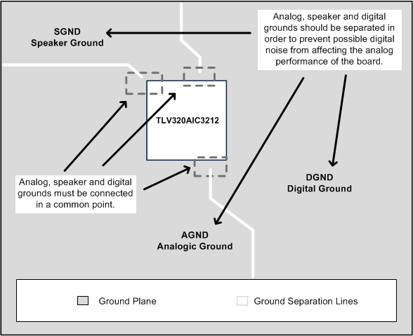
- Analog, speaker and digital grounds should be separated to prevent possible digital noise from affecting the analog performance of the board.


