SBOS755 October 2016 TLV2376 , TLV376 , TLV4376
PRODUCTION DATA.
- 1 Features
- 2 Applications
- 3 Description
- 4 Revision History
- 5 Pin Configuration and Functions
- 6 Specifications
- 7 Detailed Description
- 8 Application and Implementation
- 9 Power Supply Recommendations
- 10Layout
- 11Device and Documentation Support
- 12Mechanical, Packaging, and Orderable Information
Package Options
Mechanical Data (Package|Pins)
Thermal pad, mechanical data (Package|Pins)
Orderable Information
1 Features
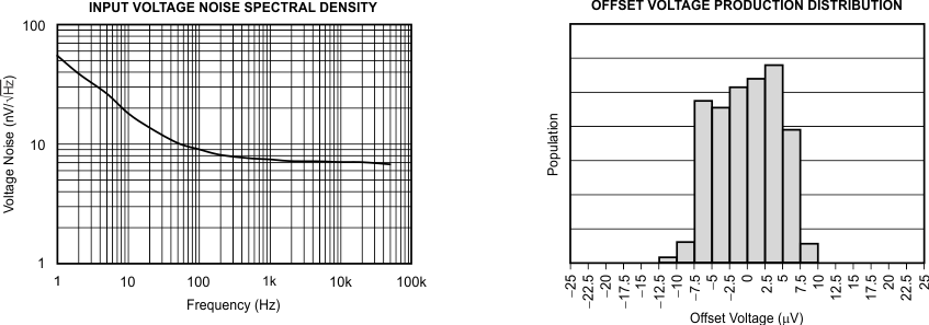
- Low Noise: 8 nV/√Hz at 1 kHz
- 0.1-Hz to 10-Hz Noise: 1.6 μVPP
- Quiescent Current: 815 μA (typical)
- Low Offset Voltage (typical):
- Single and Dual Versions: 40 μV
- Quad Version: 50 μV
- Gain Bandwidth Product: 5.5 MHz
- Rail-to-Rail Input and Output
- Single-Supply Operation
- Supply Voltage: 2.2 V to 5.5 V
- Industry-Standard Packages:
- SOT-23, SOIC, VSSOP, TSSOP
2 Applications
- Solar Inverters
- Medical Instrumentation
- ADC Buffers
- Handheld Test Equipment
- Active Filtering
- Sensor Conditioning
3 Description
The TLVx376 family represents a new generation of low-noise operational amplifiers with e-trim™, offering both excellent dc precision and ac performance. Rail-to-rail input and output, low offset (125 μV, maximum), low noise (8 nV/√Hz), a quiescent current of 1.2 mA (maximum), and a 5.5-MHz bandwidth with a fast slew rate of 2 V/μs make this family of devices very attractive for a variety of precision and portable applications. In addition, these devices have a reasonably wide supply range with excellent PSRR, making the family ideal for applications that run directly from batteries without regulation.
The TLV376 (single version) is available in SOT-23-5 and SOIC-8 packages. The TLV2376 (dual) is offered in VSSOP-8 and SOIC-8 packages. The TLV4376 (quad) is offered in a TSSOP-14 package. All versions are specified for operation from –40°C to +125°C.
Device Information(1)
| PART NUMBER | PACKAGE | BODY SIZE (NOM) |
|---|---|---|
| TLV376 | SOIC (8) | 4.90 mm × 3.91 mm |
| SOT-23 (5) | 2.90 mm × 1.60 mm | |
| TLV2376 | SOIC (8) | 4.90 mm × 3.91 mm |
| VSSOP (8) | 3.00 mm × 3.00 mm | |
| TLV4376 | PW (14) | 5.00 mm × 4.40 mm |
- For all available packages, see the package option addendum at the end of the data sheet.

4 Revision History
| DATE | REVISION | NOTES |
|---|---|---|
| October 2016 | * | Initial release. |