SNVSB04C March 2019 – December 2021 TLV4021 , TLV4031 , TLV4041 , TLV4051
PRODUCTION DATA
- 1 Features
- 2 Applications
- 3 Description
- 4 Revision History
- 5 Pin Configuration and Functions
- 6 Specifications
- 7 Typical Characteristics
- 8 Detailed Description
- 9 Application and Implementation
- 10Power Supply Recommendations
- 11Layout
- 12Device and Documentation Support
- 13Mechanical, Packaging, and Orderable Information
Package Options
Mechanical Data (Package|Pins)
Thermal pad, mechanical data (Package|Pins)
Orderable Information
9.2.1.2 Detailed Design Procedure
Configure the circuit as shown in Figure 9-4. Connect (V+) to 3.3 V which also powers the micro-controller. Resistors R1 and R2 create the under-voltage alert level of 2.0 V. When the battery voltage sags down to 2.0 V, the resistor divider voltage crosses the (VIT-) threshold of the TLV4041R1. This causes the comparator output to transition from a logic high to a logic low. The push-pull option of the TLV40x1 family is selected since the comparator operating voltage is shared with the microcontroller which is receiving the under-voltage alert signal. The TLV4041 option with the 1.2 V internal reference is selected because it is the closest internal reference option that is less than the critical under-voltage level of 2.0 V. Choosing the internal reference option that is closest to the critical under-voltage level minimizes the resistor divider ratio which optimizes the accuracy of the circuit. Error at the falling edge threshold of (VIT-) is amplified by the inverse of the resistor divider ratio. So minimizing the resistor divider ratio is a way of optimizing voltage monitoring accuracy.
Equation 1 is derived from the analysis of Figure 9-4.
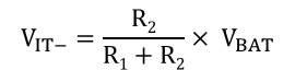
where
- R1 and R2 are the resistor values for the resistor divider connected to IN
- VBAT is the voltage source that is being monitored for an undervoltage condition.
- VIT- is the falling edge threshold where the comparator output changes state from high to low
Rearranging Equation 1 and solving for R1 yields Equation 2.
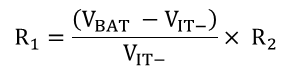
For the specific undervoltage detection of 2.0 V using the TLV4041R1, the following results are calculated.
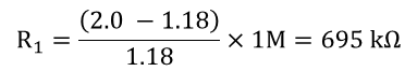
where
- R2 is set to 1 MΩ
- VBAT is set to 2.0 V
- VIT- is set to1.18 V
Choose RTOTAL (R1 + R2) such that the current through the divider is at least 100 times higher than the input bias current (IBIAS). The resistors can have high values to minimize current consumption in the circuit without adding significant error to the resistive divider.