SBVS404A April   2020  – June 2020 TLV4062 , TLV4082

PRODUCTION DATA.  

  1. Features
  2. Applications
  3. Description
    1.     Device Images
      1.      Block Diagram for TLV4062
      2.      Block Diagram for TLV4082
  4. Revision History
  5. Pin Configuration and Functions
    1.     Pin Functions
  6. Specifications
    1. 6.1 Absolute Maximum Ratings
    2. 6.2 ESD Ratings
    3. 6.3 Recommended Operating Conditions
    4. 6.4 Thermal Information
    5. 6.5 Electrical Characteristics
    6. 6.6 Timing Requirements
    7. 6.7 Typical Characteristics
  7. Detailed Description
    1. 7.1 Overview
    2. 7.2 Functional Block Diagrams
    3. 7.3 Feature Description
    4. 7.4 Device Functional Modes
      1. 7.4.1 Inputs (IN1, IN2)
      2. 7.4.2 Outputs (OUT1, OUT2)
      3. 7.4.3 Switching Threshold and Hysteresis
  8. Application and Implementation
    1. 8.1 Application Information
      1. 8.1.1 Threshold Overdrive
    2. 8.2 Typical Applications
      1. 8.2.1 Monitoring Two Separate Rails
        1. 8.2.1.1 Design Requirements
        2. 8.2.1.2 Detailed Design Procedure
        3. 8.2.1.3 Application Curve
      2. 8.2.2 Early Warning Detection
        1. 8.2.2.1 Design Requirements
        2. 8.2.2.2 Detailed Design Procedure
        3. 8.2.2.3 Application Curve
      3. 8.2.3 Additional Application Information
        1. 8.2.3.1 Pull-Up Resistor Selection
        2. 8.2.3.2 INx Capacitor
  9. Power Supply Recommendations
  10. 10Layout
    1. 10.1 Layout Guidelines
    2. 10.2 Layout Example
  11. 11Device and Documentation Support
    1. 11.1 Documentation Support
      1. 11.1.1 Related Documentation
    2. 11.2 Receiving Notification of Documentation Updates
    3. 11.3 Related Links
    4. 11.4 Support Resources
    5. 11.5 Trademarks
    6. 11.6 Electrostatic Discharge Caution
    7. 11.7 Glossary

Package Options

Mechanical Data (Package|Pins)
Thermal pad, mechanical data (Package|Pins)
Orderable Information

Application Curve

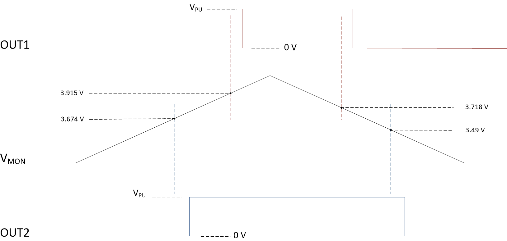
Figure 26 shows the simulated results of the early warning detection circuit. OUT2 provides the early warning alert whereas OUT1 provides the warning alert.
TLV4062 TLV4082 app_curve2.gifFigure 26. Early Warning Detection