SBOS934A August   2018  – December 2018 TLV6001-Q1 , TLV6002-Q1

PRODUCTION DATA.  

  1. Features
  2. Applications
  3. Description
    1.     CMRR and PSRR vs Temperature
  4. Revision History
  5. Pin Configuration and Functions
    1.     Pin Functions: TLV6001-Q1
    2.     Pin Functions: TLV6002-Q1
  6. Specifications
    1. 6.1 Absolute Maximum Ratings
    2. 6.2 ESD Ratings
    3. 6.3 Recommended Operating Conditions
    4. 6.4 Thermal Information: TLV6001-Q1
    5. 6.5 Thermal Information: TLV6002-Q1
    6. 6.6 Electrical Characteristics: VS = 1.8 V to 5 V (±0.9 V to ±2.75 V)
    7. 6.7 Typical Characteristics: Table of Graphs
    8. 6.8 Typical Characteristics
  7. Detailed Description
    1. 7.1 Overview
    2. 7.2 Functional Block Diagram
    3. 7.3 Feature Description
      1. 7.3.1 Operating Voltage
      2. 7.3.2 Rail-to-Rail Input
      3. 7.3.3 Rail-to-Rail Output
      4. 7.3.4 Common-Mode Rejection Ratio (CMRR)
      5. 7.3.5 Capacitive Load and Stability
      6. 7.3.6 EMI Susceptibility and Input Filtering
    4. 7.4 Device Functional Modes
    5. 7.5 Input and ESD Protection
  8. Application and Implementation
    1. 8.1 Application Information
    2. 8.2 Typical Application
      1. 8.2.1 Design Requirements
      2. 8.2.2 Detailed Design Procedure
      3. 8.2.3 Application Curve
    3. 8.3 System Examples
  9. Power Supply Recommendations
  10. 10Layout
    1. 10.1 Layout Guidelines
    2. 10.2 Layout Example: Single Channel
    3. 10.3 Layout Example: Dual Channel
  11. 11Device and Documentation Support
    1. 11.1 Documentation Support
      1. 11.1.1 Related Documentation
    2. 11.2 Related Links
    3. 11.3 Receiving Notification of Documentation Updates
    4. 11.4 Community Resources
    5. 11.5 Trademarks
    6. 11.6 Electrostatic Discharge Caution
    7. 11.7 Glossary
  12. 12Mechanical, Packaging, and Orderable Information

Package Options

Refer to the PDF data sheet for device specific package drawings

Mechanical Data (Package|Pins)
  • D|8
  • DGK|8
Thermal pad, mechanical data (Package|Pins)
Orderable Information

System Examples

When receiving low-level signals, limiting the bandwidth of the incoming signals into the system is often required. To establish this minimum bandwidth, place an RC filter at the noninverting pin of the amplifier, as Figure 23 shows.
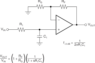
TLV6001-Q1 TLV6002-Q1 ai_single_pole_lpf_bos563.gifFigure 23. Single-Pole Low-Pass Filter

If even more attenuation is needed, a multiple pole filter is required. The Sallen-Key filter can be used for this task, as Figure 24 shows. For best results, the amplifier must have a bandwidth that is 8 to 10 times larger than the filter frequency bandwidth. Failure to follow this guideline can result in phase shift of the amplifier.
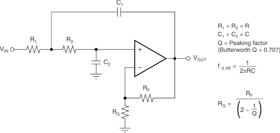
TLV6001-Q1 TLV6002-Q1 ai_2_pole_sallen_key_lpf_bos563.gifFigure 24. Two-Pole, Low-Pass, Sallen-Key Filter