SLVSEX0A March   2019  – July 2019 TLV61048

PRODUCTION DATA.  

  1. Features
  2. Applications
  3. Description
    1.     Device Images
      1.      Simplified Schematic
  4. Revision History
  5. Pin Configuration and Functions
    1.     Pin Functions
  6. Specifications
    1. 6.1 Absolute Maximum Ratings
    2. 6.2 ESD Ratings
    3. 6.3 Recommended Operating Conditions
    4. 6.4 Thermal Information
    5. 6.5 Electrical Characteristics
    6. 6.6 Typical Characteristics
  7. Detailed Description
    1. 7.1 Overview
    2. 7.2 Functional Block Diagram
    3. 7.3 Feature Description
      1. 7.3.1 Undervoltage Lockout
      2. 7.3.2 Enable and Disable
      3. 7.3.3 Soft Start
      4. 7.3.4 Frequency Select (FREQ)
    4. 7.4 Device Functional Modes
      1. 7.4.1 PWM Mode
      2. 7.4.2 PFM Mode
  8. Application and Implementation
    1. 8.1 Application Information
    2. 8.2 Typical Applications
      1. 8.2.1 12-V Output Boost Converter With External Bias
        1. 8.2.1.1 Design Requirements
        2. 8.2.1.2 Detailed Design Procedure
          1. 8.2.1.2.1 Programming the Output Voltage
          2. 8.2.1.2.2 Inductor Selection
          3. 8.2.1.2.3 Input and Output Capacitor Selection
          4. 8.2.1.2.4 Diode Rectifier Selection
        3. 8.2.1.3 Application Curves
      2. 8.2.2 14-V Output Boost Converter
        1. 8.2.2.1 Design Requirements
        2. 8.2.2.2 Detailed Design Procedure
          1. 8.2.2.2.1 Inductor Selection
          2. 8.2.2.2.2 Input and Output Capacitor Selection
  9. Power Supply Recommendations
  10. 10Layout
    1. 10.1 Layout Guidelines
    2. 10.2 Layout Example
  11. 11Device and Documentation Support
    1. 11.1 Device Support
      1. 11.1.1 Third-Party Products Disclaimer
    2. 11.2 Receiving Notification of Documentation Updates
    3. 11.3 Community Resources
    4. 11.4 Trademarks
    5. 11.5 Electrostatic Discharge Caution
    6. 11.6 Glossary
  12. 12Mechanical, Packaging, and Orderable Information

Package Options

Mechanical Data (Package|Pins)
Thermal pad, mechanical data (Package|Pins)
Orderable Information

PFM Mode

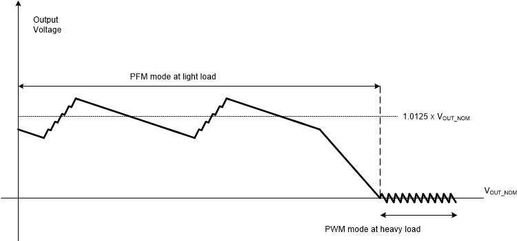
The TLV61048 integrates a power save mode with pulse frequency modulation (PFM) to improve efficiency at light load. When the load current decreases, the inductor peak current set by the output of the error amplifier declines to regulate the output voltage. When the inductor peak current hits the low limit (400 mA typical), the output voltage exceeds the set threshold voltage as the load current decreases further. When the FB voltage hits the PFM reference voltage, the TLV61048 goes into power-save mode. In the power-save mode, the device only switches when the output voltage trips below a set threshold voltage. It ramps up the output with several pulses and enters the power save mode when the output voltage exceeds the set threshold voltage.
TLV61048 pfm_SLVSEX0.gif