SLVSAK9H October 2011 – January 2017 TLV62080 , TLV62084 , TLV62084A
UNLESS OTHERWISE NOTED, this document contains PRODUCTION DATA.
- 1 Features
- 2 Applications
- 3 Description
- 4 Revision History
- 5 Device Comparison Table
- 6 Pin Configuration and Functions
- 7 Specifications
- 8 Detailed Description
- 9 Application and Implementation
- 10Power Supply Recommendations
- 11Layout
- 12Device and Documentation Support
- 13Mechanical, Packaging, and Orderable Information
Package Options
Mechanical Data (Package|Pins)
- DSG|8
Thermal pad, mechanical data (Package|Pins)
- DSG|8
Orderable Information
7 Specifications
7.1 Absolute Maximum Ratings(1)
| MIN | MAX | UNIT | ||
|---|---|---|---|---|
| Voltage range(2) | VIN, PG, VOS | – 0.3 | 7 | V |
| SW | – 0.3 | VIN + 0.3 | V | |
| SW (AC, less than 10 ns)(3) | – 3.0 | 10 | V | |
| FB | – 0.3 | 3.6 | V | |
| EN | – 0.3 | VIN + 0.3 | V | |
| Power Good Sink Current | PG | 1 | mA | |
| Operating junction temperature range, TJ | – 40 | 150 | °C | |
| Storage temperature range, Tstg | – 65 | 150 | °C | |
(1) Stresses beyond those listed under absolute maximum ratings may cause permanent damage to the device. These are stress ratings only and functional operation of the device at these or any other conditions beyond those indicated under recommended operating conditions is not implied. Exposure to absolute–maximum–rated conditions for extended periods may affect device reliability.
(2) All voltage values are with respect to network ground terminal.
(3) While switching.
7.2 ESD Ratings
| VALUE | UNIT | |||
|---|---|---|---|---|
| V(ESD) | Electrostatic discharge | Human body model (HBM) ESD stress voltage(1) | ±2000 | V |
| Charged device model (CDM) ESD stress voltage(2) | ±500 | V | ||
(1) Level listed above is the passing level per ANSI/ESDA/JEDEC JS-001. JEDEC document JEP155 states that 500-V HBM allows safe manufacturing with a standard ESD control process.
(2) Level listed above is the passing level per EIA-JEDEC JESD22-C101. JEDEC document JEP157 states that 250-V CDM allows safe manufacturing with a standard ESD control process.
7.3 Recommended Operating Conditions(1)
| MIN | TYP | MAX | UNIT | ||
|---|---|---|---|---|---|
| VIN | Input voltage range, TLV62080 | 2.5 | 6 | V | |
| VIN | Input voltage range, TLV62084, TLV62084A | 2.7 | 6 | V | |
| TJ | Operating junction temperature | –40 | 125 | °C |
(1) Refer to the Application Information section for further information.
7.4 Thermal Information
| THERMAL METRIC(1) | TLV6208x DSG (8 PINS) |
UNITS | |
|---|---|---|---|
| θJA | Junction-to-ambient thermal resistance | 59.7 | °C/W |
| θJCtop | Junction-to-case (top) thermal resistance | 70.1 | °C/W |
| θJB | Junction-to-board thermal resistance | 30.9 | °C/W |
| ψJT | Junction-to-top characterization parameter | 1.4 | °C/W |
| ψJB | Junction-to-board characterization parameter | 31.5 | °C/W |
| θJCbot | Junction-to-case (bottom) thermal resistance | 8.6 | °C/W |
(1) For more information about traditional and new thermal metrics, see the Semiconductor and IC Package Thermal Metrics application report.
7.5 Electrical Characteristics
Over recommended free-air temperature range, TA = –40°C to 85°C, typical values are at TA = 25°C (unless otherwise noted), VIN= 3.6 V.7.6 Typical Characteristics
See Typical Application for characterization setup.
space
Table 1. Table of Graphs
| FIGURE | ||
|---|---|---|
| Efficiency | Load current, VOUT = 0.9 V | Figure 1 |
| Load current, VOUT = 1.2 V | Figure 2 | |
| Load current, VOUT = 2.5 V | Figure 3 | |
| Output Voltage Accuracy | Input Voltage, VOUT = 0.9 V | Figure 4 |
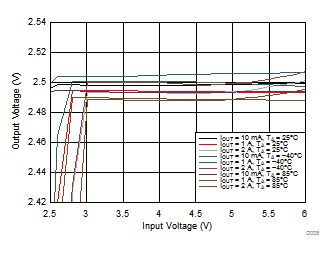
| Input Voltage, VOUT = 2.5 V | Figure 5 | |
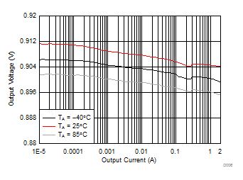
| Load current, VOUT = 0.9 V | Figure 6 | |
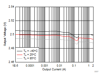
| Load current, VOUT = 2.5 V | Figure 7 | |
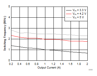
| Switching Frequency | Load current, VOUT = 2.5 V | Figure 8 |
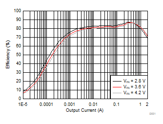
| VOUT = 0.9 V | ||
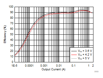
| VOUT = 2.5 V | ||
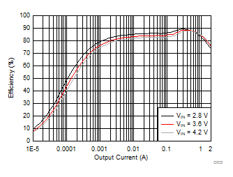
| VOUT = 1.2 V | ||
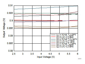
| VOUT = 0.9 V | ||
