SLVSBC1D October 2013 – October 2016 TLV62565 , TLV62566
PRODUCTION DATA.
- 1 Features
- 2 Applications
- 3 Description
- 4 Simplified Schematic
- 5 Revision History
- 6 Device Comparison Table
- 7 Pin Configuration and Functions
- 8 Specifications
- 9 Detailed Description
- 10Application and Implementation
- 11Power Supply Recommendations
- 12Layout
- 13Device and Documentation Support
- 14Mechanical, Packaging, and Orderable Information
Package Options
Mechanical Data (Package|Pins)
- DBV|5
Thermal pad, mechanical data (Package|Pins)
Orderable Information
9 Detailed Description
9.1 Overview
The TLV62565/6 device family includes two high-efficiency synchronous step-down converters. Each device operates with an adaptive on-time control scheme, which is able to dynamically adjust the on-time duration based on the input voltage and output voltage so that it can achieve relative constant frequency operation. The device operates at typically 1.5-MHz frequency pulse width modulation (PWM) at moderate to heavy load currents. Based on the VIN/VOUT ratio, a simple circuit sets the required on time for the high-side MOSFET. It makes the switching frequency relatively constant regardless of the variation of input voltage, output voltage, and load current. At the beginning of each switching cycle, the high-side switch is turned on and the inductor current ramps up to a peak current that is defined by on time and inductance. In the second phase, once the on time expires, the high-side switch is turned off while the low-side switch is turned on. The current through the inductor then decays until triggering the valley current level determined by the output of the error amplifier. Once this occurs, the on timer is set to turn the high-side switch back on again and the cycle is repeated.
The TLV62565/6 device family offers excellent load transient response with a unique fast response constant on-time valley current mode. The switching frequency changes during load transition so that the output voltage comes back in regulation faster than a traditional fixed PWM control scheme. Internal loop compensation is integrated which simplifies the design process while minimizing the number of external components. At light load currents the device automatically operates in Power Save Mode with pulse frequency modulation (PFM).
9.2 Functional Block Diagrams
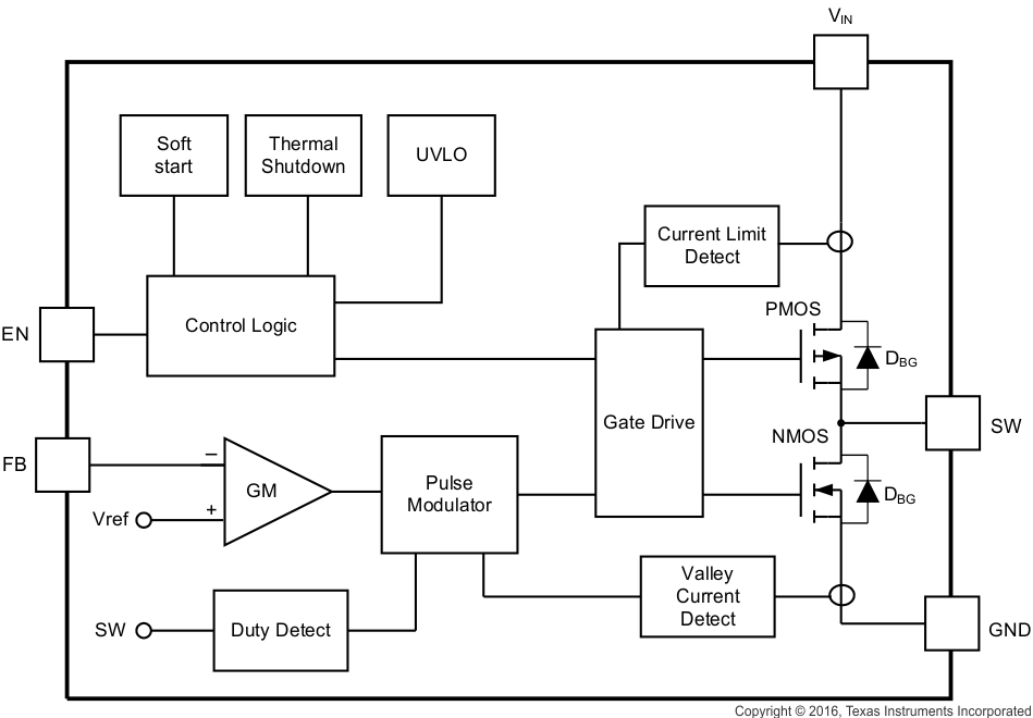
 Figure 4. TLV62565 Functional Block Diagram
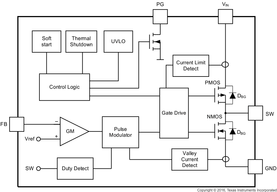
 Figure 5. TLV62566 Functional Block Diagram
9.3 Feature Description
9.3.1 Power Save Mode
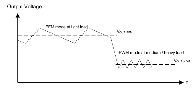
The device integrates a Power Save Mode with PFM to improve efficiency at light load, as shown in Figure 6
When the inductor current becomes discontinuous, the device enters Power Save Mode. In Power Save Mode, the FB voltage is typically 0.9% higher than the nominal value of 0.6 V. Thus the device ramps up the output voltage with several pulses, and the device stops switching when the output voltage reaches 0.9% above the nominal output voltage.
When the inductor current becomes continuous again, the device leaves Power Save Mode and the FB voltage is back to the norminal value of 0.6 V.
 Figure 6. Output Voltage in PFM/PWM Mode
9.3.2 Enabling/Disabling the Device
The TLV62565 is enabled by setting the EN input to a logic HIGH. Accordingly, a logic LOW disables the device. If the device is enabled, the internal power stage starts switching and regulates the output voltage to the set point voltage. The EN input must be terminated and should not be left floating.
9.3.3 Soft Start
After enabling the device, internal soft-start circuitry monotonically ramps up the output voltage which reaches nominal output voltage during a soft-start time of 250 µs (typical). This avoids excessive inrush current and creates a smooth output voltage rise slope. It also prevents excessive voltage drops of primary cells and rechargeable batteries with high internal impedance.
If the output voltage is not reached within the soft-start time, such as in the case of a heavy load, the converter enters regular operation. The TLV62565/6 are able to start into a pre-biased output capacitor. The converter starts with the applied bias voltage and ramps the output voltage to its nominal value.
9.3.4 Switch Current Limit
The switch current limit prevents the device from high inductor current and drawing excessive current from a battery or input voltage rail. Excessive current might occur with a heavy load or shorted output circuit condition.
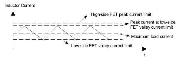
The TLV62565/6 adopt valley current control by sensing the current of the low-side FET. If the inductor current reaches the low-side FET valley current limit ILIM,LS (typical 1.7 A), the low-side FET is turned off and the high-side FET is turned on to ramp up the inductor current. The current ramping up time is controlled by the on time setting of the device, as shown in Figure 7. For example, the peak current is 1.97 A when the switch current limit is triggered with 3.6 VIN to 1.8 VOUT and 2.2-μH application.
To prevent the inductor current from running away, the devices implement an additional high-side peak current limit ILIM,HS (typical 2 A), which is shown in Figure 7. It forces to turn off the high side FET immediately once the peak inductor current reaches the threshold. Due to the internal propagation delay, the real current limit value might be higher than the static current limit in the electrical characteristics table.
 Figure 7. Switch Current Limit
9.3.5 Power Good
The TLV62566 integrates a Power Good output going low when the output voltage is below its nominal value. The Power Good output stays high impedance once the output is above 95% of the regulated voltage and is low once the output voltage falls below typically 90% of the regulated voltage. The PG pin is an open drain output and is specified to sink typically up to 0.5 mA. The Power Good output requires a pull-up resistor connected to any voltage lower than 5.5 V. When the device is off due to UVLO or thermal shutdown, the PG pin is pulled to logic low.
9.4 Device Functional Modes
9.4.1 Under Voltage Lockout
To avoid mis-operation of the device at low input voltages, under voltage lockout is implemented that shuts down the device at voltages lower than VUVLO with VHYS_UVLO hysteresis.
9.4.2 Thermal Shutdown
The device enters thermal shutdown once the junction temperature exceeds typically TJSD. Once the device temperature falls below the threshold with hysteresis, the device returns to normal operation automatically. Power Good is pulled low when thermal protection is triggered.