SLVSD89B November 2016 – November 2017 TLV62568
PRODUCTION DATA.
- 1 Features
- 2 Applications
- 3 Description
- 4 Revision History
- 5 Pin Configuration and Functions
- 6 Specifications
- 7 Detailed Description
- 8 Application and Implementation
- 9 Power Supply Recommendations
- 10Layout
- 11Device and Documentation Support
- 12Mechanical, Packaging, and Orderable Information
Package Options
Mechanical Data (Package|Pins)
Thermal pad, mechanical data (Package|Pins)
Orderable Information
1 Features
- Up to 95% Efficiency
- Low RDS(ON) Switches 150 mΩ / 100 mΩ
- 2.5-V to 5.5-V Input Voltage Range
- Adjustable Output Voltage from 0.6 V to VIN
- Power Save Mode for Light Load Efficiency
- 100% Duty Cycle for Lowest Dropout
- 35-µA Operating Quiescent Current
- 1.5-MHz Switching Frequency
- Power Good Output
- Over Current Protection
- Internal Soft Startup
- Thermal Shutdown Protection
- Available in SOT Package
- Pin-to-Pin Compatible with TLV62569
- Create a Custom Design Using the TLV62568 With the WEBENCH® Power Designer
2 Applications
- General Purpose POL Supply
- Network Video Camera
- Set Top Box
- Wireless Router
3 Description
The TLV62568 device is a synchronous step-down buck DC-DC converter optimized for high efficiency and compact solution size. The device integrates switches capable of delivering an output current up to 1 A.
At medium to heavy loads, the device operates in pulse width modulation (PWM) mode with 1.5-MHz switching frequency. At light load, the device automatically enters Power Save Mode (PSM) to maintain high efficiency over the entire load current range. In shutdown, the current consumption is reduced to less than 2 μA.
The TLV62568 provides an adjustable output voltage via an external resistor divider. An internal soft start circuit limits the inrush current during startup. Other features like over current protection, thermal shutdown protection and power good are built-in. The device is available in a SOT23 and SOT563 package.
Device Information(1)
| PART NUMBER | PACKAGE | BODY SIZE (NOM) |
|---|---|---|
| TLV62568 | SOT-23 (5) | 2.90 mm × 2.80 mm |
| TLV62568P | SOT-23 (6) | |
| TLV62568 | SOT563 (6) | 1.60 mm x 1.60 mm |
| TLV62568P | SOT563 (6) |
- For all available packages, see the orderable addendum at the end of the datasheet.
Device Comparison
| PART NUMBER | FUNCTION | PACKAGE MARKING |
|---|---|---|
| TLV62568DBV | - | 14VF |
| TLV62568PDDC | Power Good | 9X |
| TLV62568DRL | - | 18L |
| TLV62568PDRL | Power Good | 18N |
SPACER
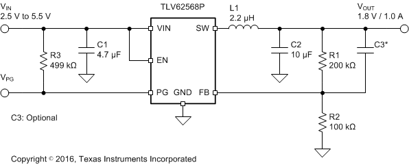
Simplified Schematic

Efficiency at 5-V Input Voltage
