SLVSD89B November 2016 – November 2017 TLV62568
PRODUCTION DATA.
- 1 Features
- 2 Applications
- 3 Description
- 4 Revision History
- 5 Pin Configuration and Functions
- 6 Specifications
- 7 Detailed Description
- 8 Application and Implementation
- 9 Power Supply Recommendations
- 10Layout
- 11Device and Documentation Support
- 12Mechanical, Packaging, and Orderable Information
Package Options
Mechanical Data (Package|Pins)
Thermal pad, mechanical data (Package|Pins)
Orderable Information
10 Layout
10.1 Layout Guidelines
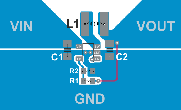
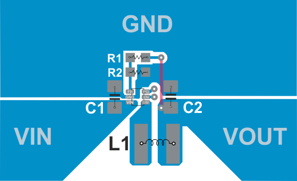
The PCB layout is an important step to maintain the high performance of the TLV62568 device.
- The input/output capacitors and the inductor should be placed as close as possible to the IC. This keeps the power traces short. Routing these power traces direct and wide results in low trace resistance and low parasitic inductance.
- The low side of the input and output capacitors must be connected properly to the power GND to avoid a GND potential shift.
- The sense traces connected to FB are signal traces. Special care should be taken to avoid noise being induced. Keep these traces away from SW nodes.
- GND layers might be used for shielding.
10.3 Thermal Considerations
Implementation of integrated circuits in low-profile and fine-pitch surface-mount packages typically requires special attention to power dissipation. Many system-dependent issues such as thermal coupling, airflow, convection surfaces, and the presence of other heat-generating components affect the power dissipation limits of a given component.
Two basic approaches for enhancing thermal performance are listed below:
- Improving the power dissipation capability of the PCB design
- Introducing airflow in the system
For more details on how to use the thermal parameters, see the application notes: Thermal Characteristics Application Notes SZZA017 and SPRA953.

