SLVSDH5B June 2016 – March 2021 TLV627432
PRODUCTION DATA
- 1 Features
- 2 Applications
- 3 Description
- 4 Revision History
- 5 Device Comparison Table
- 6 Pin Configuration and Functions
- 7 Specifications
- 8 Detailed Description
- 9 Application and Implementation
- 10Power Supply Recommendations
- 11Layout
- 12Device and Documentation Support
- 13Mechanical, Packaging, and Orderable Information
Package Options
Mechanical Data (Package|Pins)
- YFP|8
Thermal pad, mechanical data (Package|Pins)
Orderable Information
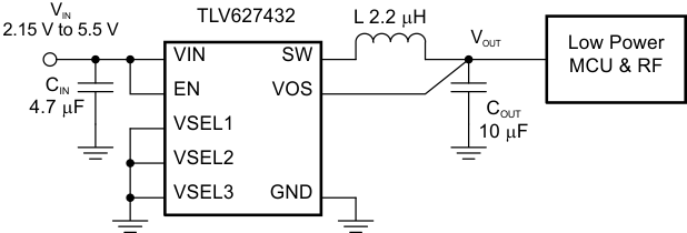
3 Description
The TLV627432 is a high
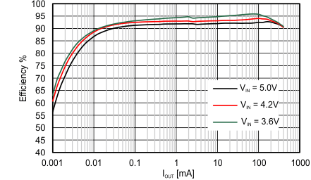
efficiency step down converter with ultra low quiescent current of typical 360 nA. The
device is optimized to operate with a 2.2-µH inductor and 10-µF output capacitor. The
device uses DCS-Control and operates with a typical switching frequency of 1.2 MHz. In
Power Save Mode the device extends the light load efficiency down to a load current
range of 10 µA and below. The TLV627432 provides an output current of 300
mA. The TLV627432 provides eight programmable output voltages between 1.2 V and
3.3 V selectable by three selection pins. The TLV627432 is optimized to provide a low
output voltage ripple and low noise using a small output capacitor. Once the input
voltage comes close to the output voltage the device enters the No Ripple 100% mode to
prevent an increase of output ripple voltage. In this operation mode, the device stops
switching and turns the high side MOSFET switch on.  Typical Application
 Efficiency
Device Information
| PART NUMBER | PACKAGE(1) | BODY SIZE (NOM) |
|---|---|---|
| TLV627432 | DSBGA (8) | 1.57 mm × 0.88 mm |
(1) For all available packages, see the orderable addendum at
the end of the data sheet.
 Typical Application
 Efficiency