SNVSAV2B January   2018  – November 2019 TLV6700

PRODUCTION DATA.  

  1. Features
  2. Applications
  3. Description
    1.     Device Images
      1.      Simplified Block Diagram
      2.      Output Response
  4. Revision History
  5. Device Comparison Table
  6. Pin Configuration and Functions
    1.     Pin Functions
  7. Specifications
    1. 7.1 Absolute Maximum Ratings
    2. 7.2 ESD Ratings
    3. 7.3 Recommended Operating Conditions
    4. 7.4 Thermal Information
    5. 7.5 Electrical Characteristics
    6. 7.6 Timing Requirements
    7. 7.7 Switching Characteristics
    8. 7.8 Typical Characteristics
  8. Detailed Description
    1. 8.1 Overview
    2. 8.2 Functional Block Diagram
    3. 8.3 Feature Description
      1. 8.3.1 Inputs (INA+, INB–)
      2. 8.3.2 Outputs (OUTA, OUTB)
      3. 8.3.3 Window Comparator
      4. 8.3.4 Immunity to Input Terminal Voltage Transients
    4. 8.4 Device Functional Modes
      1. 8.4.1 Normal Operation (VDD > UVLO)
      2. 8.4.2 Undervoltage Lockout (V(POR) < VDD < UVLO)
      3. 8.4.3 Power-On Reset (VDD < V(POR))
  9. Application and Implementation
    1. 9.1 Application Information
      1. 9.1.1 VPULLUP to a Voltage Other Than VDD
      2. 9.1.2 Monitoring VDD
      3. 9.1.3 Monitoring a Voltage Other Than VDD
    2. 9.2 Typical Application
      1. 9.2.1 Design Requirements
      2. 9.2.2 Detailed Design Procedure
        1. 9.2.2.1 Resistor Divider Selection
        2. 9.2.2.2 Pullup Resistor Selection
        3. 9.2.2.3 Input Supply Capacitor
        4. 9.2.2.4 Input Capacitors
      3. 9.2.3 Application Curves
    3. 9.3 Do's and Don'ts
  10. 10Power Supply Recommendations
  11. 11Layout
    1. 11.1 Layout Guidelines
    2. 11.2 Layout Example
  12. 12Device and Documentation Support
    1. 12.1 Device Support
      1. 12.1.1 Development Support
    2. 12.2 Receiving Notification of Documentation Updates
    3. 12.3 Community Resources
    4. 12.4 Trademarks
    5. 12.5 Electrostatic Discharge Caution
    6. 12.6 Glossary
  13. 13Mechanical, Packaging, and Orderable Information

Package Options

Mechanical Data (Package|Pins)
Thermal pad, mechanical data (Package|Pins)
Orderable Information

Window Comparator

The inverting and noninverting configuration of the comparators forms a window-comparator detection circuit using a resistor divider network, as illustrated in Figure 14 and Figure 15. The input terminals can monitor any system voltage above 400 mV with the use of a resistor divider network. The INA+ and INB– terminals monitor for undervoltage and overvoltage conditions, respectively.
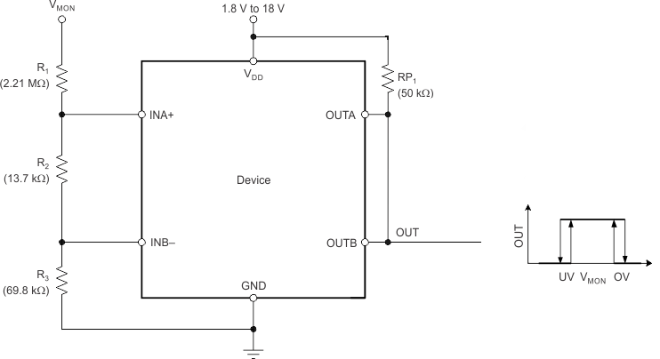
TLV6700 typ_app2_new_bvs187_Crop.pngFigure 14. Window Comparator Block Diagram
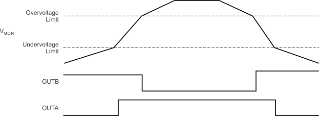
TLV6700 tim2_slvsci7.gifFigure 15. Window Comparator Timing Diagram