SBOS865B January   2018  – November 2019 TLV6703

PRODUCTION DATA.  

  1. Features
  2. Applications
  3. Description
    1.     Device Images
      1.      Simplified Block Diagram
  4. Revision History
  5. Device Comparison Table
  6. Pin Configuration and Functions
    1.     Pin Functions
  7. Specifications
    1. 7.1 Absolute Maximum Ratings
    2. 7.2 ESD Ratings
    3. 7.3 Recommended Operating Conditions
    4. 7.4 Thermal Information
    5. 7.5 Electrical Characteristics
    6. 7.6 Timing Requirements
    7. 7.7 Switching Characteristics
    8. 7.8 Typical Characteristics
  8. Detailed Description
    1. 8.1 Overview
    2. 8.2 Functional Block Diagram
    3. 8.3 Feature Description
      1. 8.3.1 Input Pin (SENSE)
      2. 8.3.2 Output Pin (OUT)
      3. 8.3.3 Immunity to Input-Pin Voltage Transients
    4. 8.4 Device Functional Modes
      1. 8.4.1 Normal Operation (VDD > UVLO)
      2. 8.4.2 Undervoltage Lockout (V(POR) < VDD < UVLO)
      3. 8.4.3 Power-On Reset (VDD < V(POR))
  9. Application and Implementation
    1. 9.1 Application Information
      1. 9.1.1 VPULLUP to a Voltage Other Than VDD
      2. 9.1.2 Monitoring VDD
      3. 9.1.3 Monitoring a Voltage Other Than VDD
    2. 9.2 Typical Application
      1. 9.2.1 Design Requirements
      2. 9.2.2 Detailed Design Procedure
        1. 9.2.2.1 Resistor Divider Selection
        2. 9.2.2.2 Pullup Resistor Selection
        3. 9.2.2.3 Input Supply Capacitor
        4. 9.2.2.4 Sense Capacitor
      3. 9.2.3 Application Curves
    3. 9.3 Dos and Don'ts
  10. 10Power-Supply Recommendations
  11. 11Layout
    1. 11.1 Layout Guidelines
    2. 11.2 Layout Example
  12. 12Device and Documentation Support
    1. 12.1 Device Support
      1. 12.1.1 Development Support
    2. 12.2 Receiving Notification of Documentation Updates
    3. 12.3 Community Resources
    4. 12.4 Trademarks
    5. 12.5 Electrostatic Discharge Caution
    6. 12.6 Glossary
  13. 13Mechanical, Packaging, and Orderable Information

Package Options

Mechanical Data (Package|Pins)
Thermal pad, mechanical data (Package|Pins)
Orderable Information

Pin Configuration and Functions

DDC Package
SOT-23-6
Top View
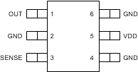
TLV6703 po_ddc_bvs271.gif
DSE Package
WSON-6
Top View
TLV6703 po_dse_bvs271.gif

Pin Functions

PIN I/O DESCRIPTION
NAME DDC DSE
GND 2, 4, 6 1, 3, 5 Connect all three pins to ground.
OUT 1 6 O SENSE comparator has an open-drain output. OUT is driven low when SENSE is below (VIT-). OUT goes high when SENSE returns above the respective threshold (VIT+).
SENSE 3 4 I This pin is connected to the voltage to be monitored with the use of an external resistor divider. When the voltage at this pin drops below the threshold voltage (VIT-), OUT is driven low.
VDD 5 2 I Supply voltage input. Connect a 1.8-V to 18-V supply to VDD to power the device. Good analog design practice is to place a 0.1-µF ceramic capacitor close to this pin.