SLVSA61H February 2010 – August 2016
PRODUCTION DATA.
- 1 Features
- 2 Applications
- 3 Description
- 4 Revision History
- 5 Pin Configuration and Functions
- 6 Specifications
- 7 Detailed Description
- 8 Application and Implementation
- 9 Power Supply Recommendations
- 10Layout
- 11Device and Documentation Support
- 12Mechanical, Packaging, and Orderable Information
Package Options
Mechanical Data (Package|Pins)
- DCK|5
Thermal pad, mechanical data (Package|Pins)
Orderable Information
8 Application and Implementation
NOTE
Information in the following applications sections is not part of the TI component specification, and TI does not warrant its accuracy or completeness. TI’s customers are responsible for determining suitability of components for their purposes. Customers should validate and test their design implementation to confirm system functionality.
8.1 Application Information
The TLV700xx-Q1 belongs to a new family of next-generation value LDO regulators. The device consumes low quiescent current and delivers excellent line and load transient performance. These characteristics, combined with low noise, very good PSRR with little (VIN – VOUT) headroom, make this device ideal for RF portable applications. This family of regulators offers subband-gap output voltages down to 0.7 V, current limit, and thermal protection, and is specified from –40°C to 125°C.
8.1.1 Input and Output Capacitor Requirements
Recommended capacitors are 1.0-μF X5R- and X7R-type ceramic because these capacitors have minimal variation in value and equivalent series resistance (ESR) over temperature.
However, the TLV700xx-Q1 is designed to be stable with an effective capacitance of 0.1 μF or larger at the output. Thus, the device is stable with capacitors of other dielectric types as well, as long as the effective capacitance under operating bias voltage and temperature is greater than 0.1 μF. This effective capacitance refers to the capacitance that the LDO sees under operating bias voltage and temperature conditions; that is, the capacitance after taking both bias voltage and temperature derating into consideration. In addition to allowing the use of cheaper dielectrics, this capability of being stable with 0.1-μF effective capacitance also enables the use of smaller-footprint capacitors that have higher derating in size- and space-constrained applications.
Note that using a 0.1-μF rated capacitor at the output of the LDO does not ensure stability because the effective capacitance under the specified operating conditions would be less than 0.1 μF. Maximum ESR should be less than 200 mΩ.
Although an input capacitor is not required for stability, it is good analog design practice to connect a 0.1-μF to 1-μF, low-ESR capacitor across the IN pin and GND in of the regulator. This capacitor counteracts reactive input sources and improves transient response, noise rejection, and ripple rejection. A higher-value capacitor may be necessary if large, fast-rise-time load transients are anticipated, or if the device is not located close to the power source. If source impedance is more than 2 Ω, a 0.1-μF input capacitor may be necessary to ensure stability.
8.1.2 Transient Response
As with any regulator, increasing the size of the output capacitor reduces over- and undershoot magnitude but increases the duration of the transient response.
8.1.3 Thermal Information
Thermal protection disables the output when the junction temperature rises to approximately 160°C, allowing the device to cool. When the junction temperature cools to approximately 140°C, the output circuitry is again enabled. Depending on power dissipation, thermal resistance, and ambient temperature, the thermal protection circuit may cycle on and off. This cycling limits the dissipation of the regulator, protecting it from damage as a result of overheating.
Any tendency to activate the thermal protection circuit indicates excessive power dissipation or an inadequate heatsink. For reliable operation, junction temperature should be limited to 125°C maximum. To estimate the margin of safety in a complete design (including heatsink), increase the ambient temperature until the thermal protection is triggered; use worst-case loads and signal conditions. For good reliability, thermal protection should trigger at least 35°C above the maximum expected ambient condition of the particular application. This configuration produces a worst-case junction temperature of 125°C at the highest expected ambient temperature and worst-case load.
The internal protection circuitry of the TLV700xx-Q1 has been designed to protect against overload conditions. It was not intended to replace proper heatsinking. Continuously running the TLV700xx-Q1 into thermal shutdown degrades device reliability.
8.2 Typical Application
The TLV700xx-Q1 devices are 200-mA, low quiescent current, low noise, high PSRR, fast-start-up LDO linear regulators with excellent line and load transient response. The TLV700xxEVM-503 evaluation module (EVM) helps designers evaluate the operation and performance of the TLV700xx-Q1 family.
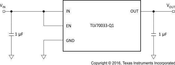
Figure 22 shows a typical application for the TLV70033-Q1 device.
 Figure 22. TLV70033-Q1 Typical Application
8.2.1 Design Requirements
Table 1 shows example design parameters and values for this typical application.
Table 1. Design Parameters
| PARAMETER | VALUE |
|---|---|
| Input voltage range | 2 V to 5.5 V |
| Output voltage | 1.2 V, 2.5 V, 3 V, 3.3 V |
| Output current rating | 200 mA |
| Effective output capacitor range | >0.1 µF |
| Maximum output capacitor ESR range | <200 mΩ |
8.2.2 Detailed Design Procedure
8.2.2.1 Input Capacitance
Although not required for stability, connecting a 0.1-µF to 1-µF low-ESR capacitor across the IN pin and GND in the regulator is good analog design practice.
8.2.2.2 Output Capacitance
Effect capacitance of 0.1 µF or larger is required to ensure stable operation. The maximum ESR must be less than 200 mΩ.
8.2.2.3 Thermal Calculation
See Equation 1 for thermal calculation.

where:
- PD = continuous power dissipation
- IOUT = output current
- VIN = input voltage
- VOUT = output voltage
- Because IQ << IOUT, the term IQ x VIN is always ignored.
For a device under operation at a given ambient air temperature (TA), use Equation 2 to calculate the junction temperature (TJ).

where:
Use Equation 3 to calculate the rise in junction temperature because of power dissipation.

For a given maximum junction temperature (TJmax), use Equation 4 to calculate the maximum ambient air temperature (TAmax) at which the device can operate.

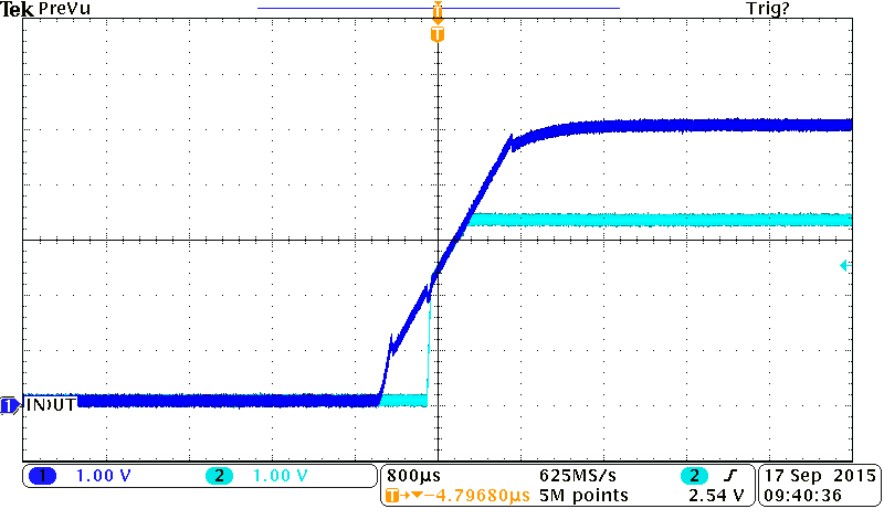
8.2.3 Application Curve
