SLVSA61H February   2010  – August 2016

PRODUCTION DATA.  

  1. Features
  2. Applications
  3. Description
  4. Revision History
  5. Pin Configuration and Functions
  6. Specifications
    1. 6.1 Absolute Maximum Ratings
    2. 6.2 ESD Ratings
    3. 6.3 Recommended Operating Conditions
    4. 6.4 Thermal Information
    5. 6.5 Electrical Characteristics
    6. 6.6 Typical Characteristics
  7. Detailed Description
    1. 7.1 Overview
    2. 7.2 Functional Block Diagram
    3. 7.3 Feature Description
      1. 7.3.1 Internal Current Limit
      2. 7.3.2 Shutdown
      3. 7.3.3 Dropout Voltage
      4. 7.3.4 Undervoltage Lockout (UVLO)
    4. 7.4 Device Functional Modes
      1. 7.4.1 Operation With VIN Less than 2 V
      2. 7.4.2 Operation With VIN Greater than 2 V
  8. Application and Implementation
    1. 8.1 Application Information
      1. 8.1.1 Input and Output Capacitor Requirements
      2. 8.1.2 Transient Response
      3. 8.1.3 Thermal Information
    2. 8.2 Typical Application
      1. 8.2.1 Design Requirements
      2. 8.2.2 Detailed Design Procedure
        1. 8.2.2.1 Input Capacitance
        2. 8.2.2.2 Output Capacitance
        3. 8.2.2.3 Thermal Calculation
      3. 8.2.3 Application Curve
  9. Power Supply Recommendations
  10. 10Layout
    1. 10.1 Layout Guidelines
    2. 10.2 Layout Example
  11. 11Device and Documentation Support
    1. 11.1 Related Links
    2. 11.2 Receiving Notification of Documentation Updates
    3. 11.3 Community Resources
    4. 11.4 Trademarks
    5. 11.5 Electrostatic Discharge Caution
    6. 11.6 Glossary
  12. 12Mechanical, Packaging, and Orderable Information

Package Options

Mechanical Data (Package|Pins)
Thermal pad, mechanical data (Package|Pins)
Orderable Information

10 Layout

10.1 Layout Guidelines

When laying out the board for the TLV700xx-Q1, TI recommends that the board be designed with separate ground planes for VIN and VOUT which are only connected at the GND pin of the device. Input and output capacitors should be placed as close to the device pins as possible. Also, the ground connection for the bypass capacitor must be connected directly to the GND pin of the device. Improve the PSRR output noise, and transient-response performance of the TLV700xx-Q1 by following these layout guidelines.

10.2 Layout Example
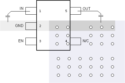
TLV70012A-Q1 TLV70025-Q1 TLV70030-Q1 TLV70033-Q1 layout_example_slvsa61.gif Figure 24. TLV700xx-Q1 Layout Example