SNOSDA5D May 2020 – February 2023 TLV7031-Q1 , TLV7032-Q1 , TLV7034-Q1 , TLV7041-Q1 , TLV7042-Q1 , TLV7044-Q1
PRODUCTION DATA
- 1 Features
- 2 Applications
- 3 Description
- 4 Revision History
- 5 Pin Configuration and Functions
-
6 Specifications
- 6.1 Absolute Maximum Ratings
- 6.2 ESD Ratings
- 6.3 Recommended Operating Conditions
- 6.4 Thermal Information (Single)
- 6.5 Thermal Information (Dual)
- 6.6 Thermal Information (Quad)
- 6.7 Electrical Characteristics
- 6.8 Switching Characteristics
- 6.9 Electrical Characteristics (Dual)
- 6.10 Switching Characteristics (Dual)
- 6.11 Electrical Characteristics (Quad)
- 6.12 Switching Characteristics (Quad)
- 6.13 Timing Diagrams
- 6.14 Typical Characteristics
- 7 Detailed Description
- 8 Application and Implementation
- 9 Power Supply Recommendations
- 10Layout
- 11Device and Documentation Support
- 12Mechanical, Packaging, and Orderable Information
Package Options
Mechanical Data (Package|Pins)
Thermal pad, mechanical data (Package|Pins)
Orderable Information
3 Description
The TLV703x-Q1/TLV704x-Q1 are low-voltage, nanopower comparators with rail-to-rail inputs. These comparators are applicable for space-critical and power conscious designs like infotainment, telematics, and head unit applications.
The TLV703x-Q1 and TLV704x-Q1 offer an excellent combination of power and speed. The benefit of fast response time at nanopower enables power-conscious systems to monitor and respond quickly to fault conditions. With an operating voltage range of 1.6 V to 6.5 V, these comparators are compatible with 1.8 V, 3 V, and 5 V systems.
The TLV703x-Q1 and TLV704x-Q1 also ensure no output phase inversion with overdriven inputs and internal hysteresis, so engineers can use this family of comparators for precision voltage monitoring in harsh, noisy environments where slow-moving input signals must be converted into clean digital outputs.
The TLV703x-Q1 have a push-pull output stage capable of sinking and sourcing milliamps of current. The TLV704x-Q1 have an open-drain output stage that can be pulled beyond VCC.
| PART NUMBERS | PACKAGE (PINS) (1) | BODY SIZE (NOM) |
|---|---|---|
| TLV7031-Q1, TLV7041-Q1 | SC70 (5) | 2.00 mm × 1.25 mm |
| SOT-23 (5) | 2.90 mm × 1.60 mm | |
| TLV7032-Q1, TLV7042-Q1 | VSSOP (8) | 3.00 mm x 3.00 mm |
| SOT-23 (8) | 2.90 mm x 1.60 mm | |
| TLV7034-Q1, TLV7044-Q1 | TSSOP (14) | 4.40 mm x 5.00 mm |
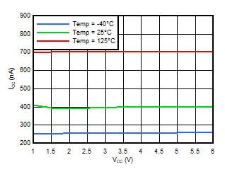
 ICC vs. VCC
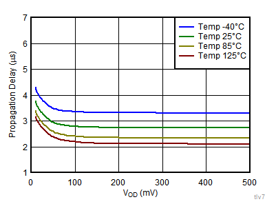
 Propagation Delay vs. Input Overdrive