SBVS176B October 2011 – April 2016 TLV717P
PRODUCTION DATA.
- 1 Features
- 2 Applications
- 3 Description
- 4 Revision History
- 5 Pin Configuration and Functions
- 6 Specifications
- 7 Detailed Description
- 8 Application and Implementation
- 9 Power Supply Recommendations
- 10Layout
- 11Device and Documentation Support
- 12Mechanical, Packaging, and Orderable Information
Package Options
Mechanical Data (Package|Pins)
- DQN|4
Thermal pad, mechanical data (Package|Pins)
- DQN|4
Orderable Information
1 Features
See the Package Option Addendum at the end of this document for a complete list of available voltage options.See2 Applications
3 Description
The TLV717P series of low-dropout (LDO) linear regulators are low quiescent current LDOs with excellent line and load transient performance and are designed for power-sensitive applications. These devices provide a typical accuracy of 0.5%.
The TLV717P series offer current foldback that throttles down the output current with a decrease in load resistance. The typical value at which current foldback initiates is 350 mA; the typical value of the output short current limit value is 40 mA.
Furthermore, these devices are stable with an effective output capacitance of only 0.1 µF. This feature enables the use of cost-effective capacitors that have higher bias voltages and temperature derating. The devices regulate to specified accuracy with no output load.
The TLV717P series is available in a 1-mm × 1-mm DQN package that makes them ideal for hand-held applications. The TLV717P provides an active pulldown circuit to quickly discharge output loads.
Device Information(1)
| PART NUMBER | PACKAGE | BODY SIZE (NOM) |
|---|---|---|
| TLV717P | X2SON (4) | 1.00 mm × 1.00 mm |
- For all available packages, see the orderable addendum at the end of the data sheet.
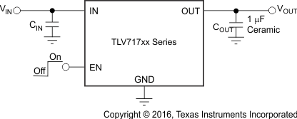
Typical Application Circuit
