SBVS235C October   2014  – July 2019 TLV733P

PRODUCTION DATA.  

  1. Features
  2. Applications
  3. Description
    1.     Device Images
      1.      Typical Application Circuit
      2.      Dropout Voltage vs Output Current
  4. Revision History
  5. Pin Configuration and Functions
    1.     Pin Functions
  6. Specifications
    1. 6.1 Absolute Maximum Ratings
    2. 6.2 ESD Ratings
    3. 6.3 Recommended Operating Conditions
    4. 6.4 Thermal Information
    5. 6.5 Electrical Characteristics
    6. 6.6 Typical Characteristics
  7. Detailed Description
    1. 7.1 Overview
    2. 7.2 Functional Block Diagram
    3. 7.3 Feature Description
      1. 7.3.1 Undervoltage Lockout (UVLO)
      2. 7.3.2 Shutdown and Output Enable
      3. 7.3.3 Internal Foldback Current Limit
      4. 7.3.4 Thermal Shutdown
    4. 7.4 Device Functional Modes
      1. 7.4.1 Normal Operation
      2. 7.4.2 Dropout Operation
      3. 7.4.3 Disabled
  8. Application and Implementation
    1. 8.1 Application Information
      1. 8.1.1 Input and Output Capacitor Selection
      2. 8.1.2 Dropout Voltage
      3. 8.1.3 Power Dissipation
    2. 8.2 Typical Applications
      1. 8.2.1 DC-DC Converter Post Regulation
        1. 8.2.1.1 Design Requirements
        2. 8.2.1.2 Design Considerations
        3. 8.2.1.3 Application Curve
      2. 8.2.2 Capacitor-Free Operation from Battery Input Supply
        1. 8.2.2.1 Design Requirements
        2. 8.2.2.2 Design Considerations
        3. 8.2.2.3 Application Curve
  9. Power Supply Recommendations
  10. 10Layout
    1. 10.1 Layout Guidelines
    2. 10.2 Layout Examples
  11. 11Device and Documentation Support
    1. 11.1 Device Support
      1. 11.1.1 Development Support
        1. 11.1.1.1 Evaluation Module
      2. 11.1.2 Device Nomenclature
    2. 11.2 Documentation Support
      1. 11.2.1 Related Documentation
    3. 11.3 Receiving Notification of Documentation Updates
    4. 11.4 Community Resources
    5. 11.5 Trademarks
    6. 11.6 Electrostatic Discharge Caution
    7. 11.7 Glossary
  12. 12Mechanical, Packaging, and Orderable Information

Package Options

Refer to the PDF data sheet for device specific package drawings

Mechanical Data (Package|Pins)
  • DBV|5
  • DQN|4
Thermal pad, mechanical data (Package|Pins)
Orderable Information

Typical Characteristics

at operating temperature range (TJ = –40°C to +125°C), VIN = VOUT(nom) + 0.5 V or 2.0 V (whichever is greater), IOUT = 1 mA, VEN = VIN, and CIN = COUT = 1 µF (unless otherwise noted)
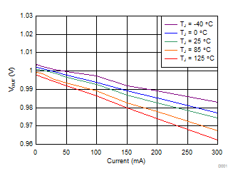
TLV733P D001_sbvs235.gif
TLV73310PDBV
Figure 1. 1.0-V Load Regulation vs IOUT and Temperature
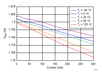
TLV733P D002_sbvs235.gif
TLV73318PDBV
Figure 3. 1.8-V Load Regulation vs IO and Temperature
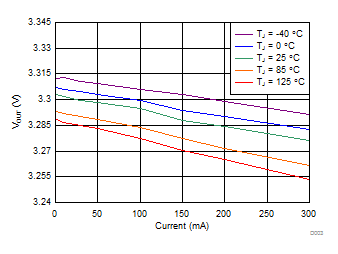
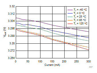
TLV733P D003_sbvs235.gif
TLV73333PDBV
Figure 5. 3.3-V Load Regulation vs IOUT and Temperature
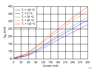
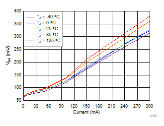
TLV733P D024_sbvs235.gif
TLV73312PDBV
Figure 7. 1.2-V Dropout Voltage vs IOUT and Temperature
TLV733P D008_sbvs235.gif
TLV73318PDBV
Figure 9. 1.8-V Dropout Voltage vs IOUT and Temperature
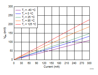
TLV733P D009_sbvs235.gif
TLV73333PDBV
Figure 11. 3.3-V Dropout Voltage vs IOUT and Temperature
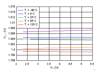
TLV733P D019_sbvs235.gif
TLV73318PDBV
Figure 13. 1.8-V Regulation vs VIN (Line Regulation) and Temperature
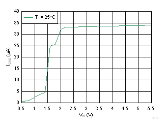
TLV733P D013_sbvs235.gif
Figure 15. Ground Pin Current vs VIN
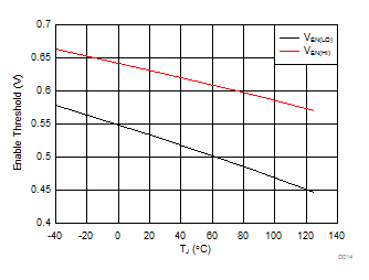
TLV733P D014_sbvs235.gif
Figure 17. Enable Threshold vs Temperature
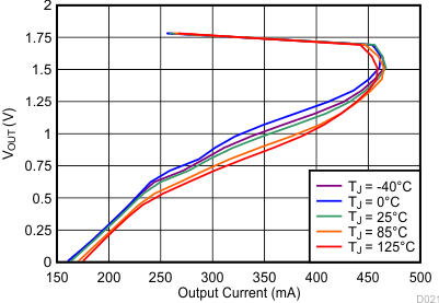
TLV733P D021_sbvs235.gif
TLV73318PDBV
Figure 19. 1.8-V Foldback Current Limit vs
IOUT and Temperature
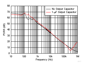
TLV733P D017_sbvs235.gif
TLV73318PDQN, IOUT = 300 mA
Figure 21. Power-Supply Rejection Ratio vs Frequency
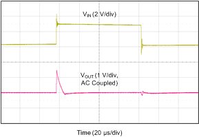
TLV733P LineTrans10mA.gif
TLV73318PDBV, IOUT = 10 mA, 1-µF output capacitor
Figure 23. Line Transient
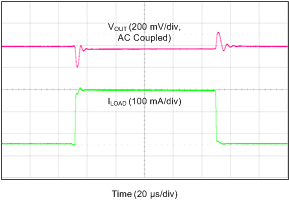
TLV733P LoadTranswcap1p0.gif
TLV73310PDBV, VIN = 2.0 V, 1-µF output capacitor, output current slew rate = 0.25 A/µs
Figure 25. 1.0-V, 50-mA to 300-mA Load Transient
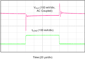
TLV733P LoadTranswcap.gif
TLV73333PDBV, VIN = 3.8 V,1-µF output capacitor, output current slew rate = 0.25 A/µs
Figure 27. 3.3 V, 50-mA to 300-mA Load Transient
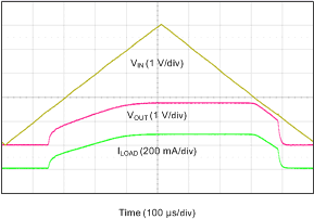
TLV733P Triangle.gif
TLV73318PDBV, RL = 6.2 Ω, VEN = VIN, 1-µF output capacitor
Figure 29. VIN Power-Up and Power-Down
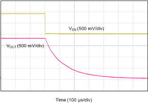
TLV733P Shutdown.gif
TLV73318PDBV, IOUT = 300 mA, 1-µF output capacitor
Figure 31. Shutdown Response with Enable
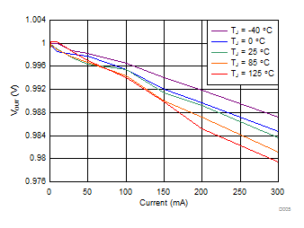
TLV733P D005_sbvs235.gif
TLV73310PDQN
Figure 2. 1.0-V Load Regulation vs IOUT and Temperature
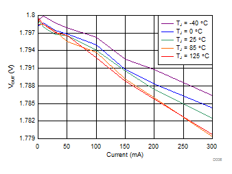
TLV733P D006_sbvs235.gif
TLV73318PDQN
Figure 4. 1.8-V Load Regulation vs IOUT and Temperature
TLV733P D007_sbvs235.gif
TLV73333PDQN
Figure 6. 3.3-V Load Regulation vs IOUT and Temperature
TLV733P D025_sbvs235.gif
TLV73312PDQN
Figure 8. 1.2-V Dropout Voltage vs IOUT and Temperature
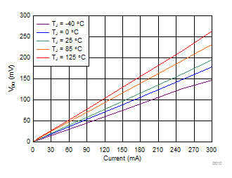
TLV733P D010_sbvs235.gif
TLV73318PDQN
Figure 10. 1.8-V Dropout Voltage vs IOUT and Temperature
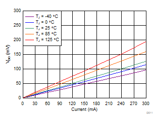
TLV733P D011_sbvs235.gif
TLV73333PDQN
Figure 12. 3.3-V Dropout Voltage vs IOUT and Temperature
TLV733P D012_sbvs235.gif
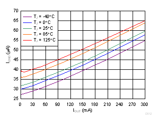
Figure 14. Ground Pin Current vs IOUT and Temperature
TLV733P D015_sbvs235.gif
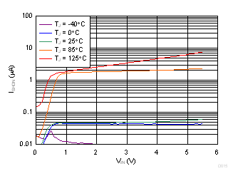
IOUT = 0 mA
Figure 16. Shutdown Current vs VIN and Temperature
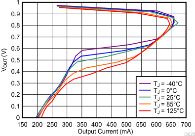
TLV733P D023_sbvs235.gif
TLV73310PDBV
Figure 18. 1.0-V Foldback Current Limit vs
IOUT and Temperature
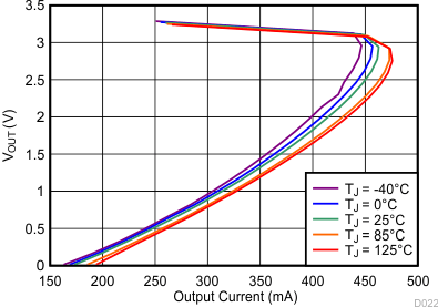
TLV733P D022_sbvs235.gif
TLV73333PDBV
Figure 20. 3.3-V Foldback Current Limit vs
IOUT and Temperature
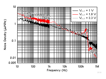
TLV733P D016_sbvs235.gif
IOUT = 300 mA
Figure 22. Output Spectral Noise Density
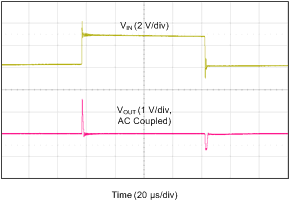
TLV733P LineTrans300mA.gif
TLV73318PDBV, IOUT = 300 mA, 1-µF output capacitor
Figure 24. Line Transient
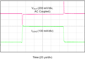
TLV733P LoadTranswocap1p0.gif
TLV73310PDBV, VIN = 2.0 V, no output capacitor, output current slew rate = 0.25 A/µs
Figure 26. 1.0 V, 50-mA to 300-mA Load Transient
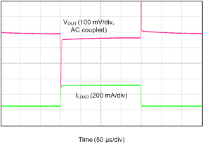
TLV733P LoadTransnocap.gif
TLV73333PDBV, VIN = 3.8 V, no output capacitor, output current slew rate = 0.25 A/µs
Figure 28. 3.3 V, 50-mA to 300-mA Load Transient
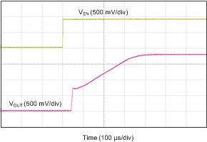
TLV733P Enstartup1p8.gif
TLV73318PDBV, RL = 6.2 Ω, 1-µF output capacitor
Figure 30. Startup with EN
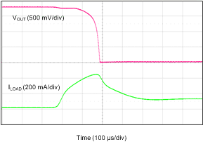
TLV733P Current_Limit.gif
TLV73318PDBV, 1-µF output capacitor
Figure 32. Foldback Current Limit Response