SBVS309A July   2017  – September 2018 TLV741P

PRODUCTION DATA.  

  1. Features
  2. Applications
  3. Description
    1.     Device Images
      1.      Typical Application Circuit
      2.      Dropout Voltage vs Output Current
  4. Revision History
  5. Pin Configuration and Functions
    1.     Pin Functions
  6. Specifications
    1. 6.1 Absolute Maximum Ratings
    2. 6.2 ESD Ratings
    3. 6.3 Recommended Operating Conditions
    4. 6.4 Thermal Information
    5. 6.5 Electrical Characteristics
    6. 6.6 Typical Characteristics
  7. Detailed Description
    1. 7.1 Overview
    2. 7.2 Functional Block Diagram
    3. 7.3 Feature Description
      1. 7.3.1 Undervoltage Lockout (UVLO)
      2. 7.3.2 Shutdown
      3. 7.3.3 Foldback Current Limit
      4. 7.3.4 Thermal Protection
    4. 7.4 Device Functional Modes
      1. 7.4.1 Normal Operation
      2. 7.4.2 Dropout Operation
      3. 7.4.3 Disabled
  8. Application and Implementation
    1. 8.1 Application Information
      1. 8.1.1 Input and Output Capacitor Considerations
      2. 8.1.2 Dropout Voltage
      3. 8.1.3 Transient Response
    2. 8.2 Typical Application
      1. 8.2.1 Design Requirements
      2. 8.2.2 Detailed Design Procedure
      3. 8.2.3 Application Curves
    3. 8.3 What to Do and What Not to Do
  9. Power Supply Recommendations
  10. 10Layout
    1. 10.1 Layout Guidelines
      1. 10.1.1 Board Layout Recommendations to Improve PSRR and Noise Performance
    2. 10.2 Layout Examples
    3. 10.3 Power Dissipation
  11. 11Device and Documentation Support
    1. 11.1 Documentation Support
      1. 11.1.1 Related Documentation
    2. 11.2 Receiving Notification of Documentation Updates
    3. 11.3 Community Resources
    4. 11.4 Trademarks
    5. 11.5 Electrostatic Discharge Caution
    6. 11.6 Glossary
  12. 12Mechanical, Packaging, and Orderable Information

Package Options

Mechanical Data (Package|Pins)
Thermal pad, mechanical data (Package|Pins)
Orderable Information

Typical Characteristics

over operating temperature range TJ = –40°C to +125°C, VIN = VOUT(nom) + 0.5 V or 2 V (whichever is greater), IOUT = 10 mA, VEN = VIN, COUT = 1 µF, and VOUT(nom) = 1.8 V (unless otherwise noted). Typical values are at TJ = 25°C.
TLV741P D001_new_SBVS195.gif
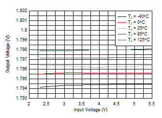
Figure 1. 1.8-V Line Regulation vs VIN and Temperature
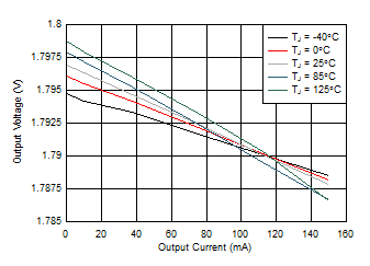
TLV741P D003_SBVS195.gif
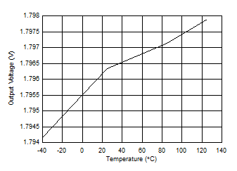
Figure 3. 1.8-V Output Voltage Over Temperature
TLV741P D005_new_SBVS195.gif
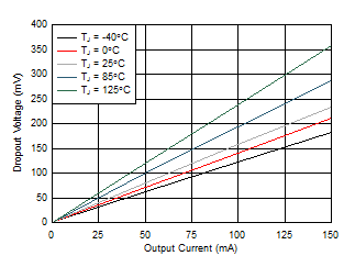
Figure 5. 3.3-V Dropout Voltage vs IOUT and Temperature
TLV741P D007_SBVS195.gif
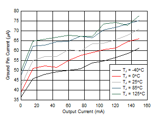
Figure 7. Ground Pin Current vs IOUT and Temperature
TLV741P D009_new_SBVS195.gif
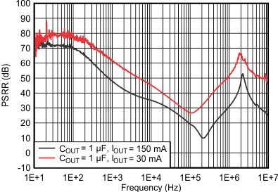
Figure 9. Power-Supply Rejection Ratio Over COUT
TLV741P D011_SBVS195.gif
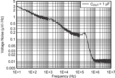
COUT = 1 µF
Figure 11. Output Spectral Noise Density
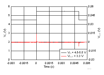
TLV741P D012_SBVS309.gif
IOUT = 1 mA
Figure 13. Line Transient
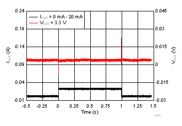
TLV741P D014_SBVS309.gif
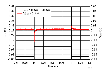
IOUT = 0 mA - 20 mA VOUT = 3.3 V
Figure 15. Load Transient
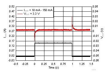
TLV741P D016_SBVS309.gif
IOUT = 10 mA - 150 mA VOUT = 3.3 V
Figure 17. Load Transient
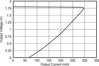
TLV741P G011_BVS195.gif
TLV74118P
Figure 19. 1.8-V Output Voltage vs Output Current
(Foldback Current Limit)
TLV741P G022_BVS195.gif
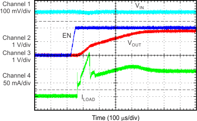
VIN = 2.3 V VOUT = 1.8 V CIN = 1 µF
COUT = 10 µF IOUT = 90 mA TLV74118P
from design
Figure 21. Start-Up With EN
TLV741P D002_SBVS195.gif
Figure 2. 1.8-V Load Regulation vs IOUT and Temperature
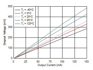
TLV741P D004_new_SBVS195.gif
Figure 4. 1.8-V Dropout Voltage vs IOUT and Temperature
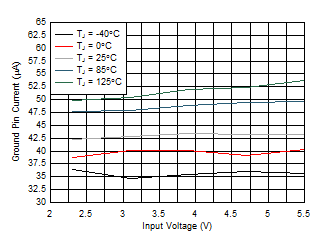
TLV741P D006_SBVS195.gif
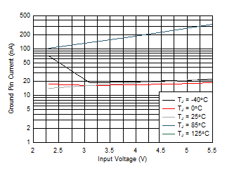
Figure 6. Ground Pin Current vs VIN and Temperature
TLV741P D008_SBVS195.gif
Figure 8. Shutdown Current vs VIN and Temperature
TLV741P D010_SBVS195.gif
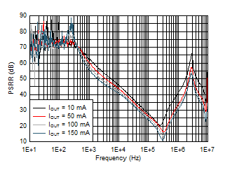
Figure 10. Power-Supply Rejection Ratio Over IOUT
TLV741P D011_SBVS309.gif
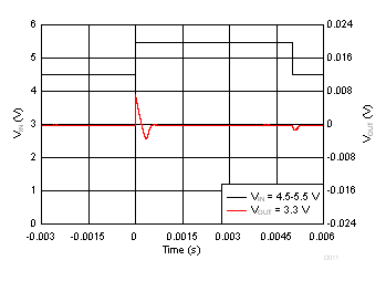
IOUT = 0 mA
Figure 12. Line Transient
TLV741P D013_SBVS309.gif
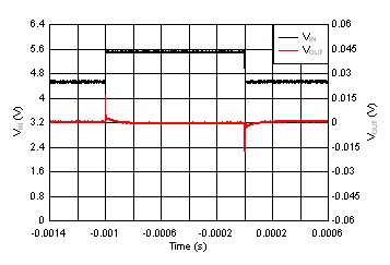
IOUT = 150 mA
Figure 14. Line Transient
TLV741P D015_SBVS309.gif
Figure 16. Load Transient
TLV741P G010_BVS195.gif
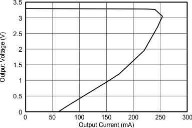
TLV74133P
Figure 18. 3.3-V Output Voltage vs Output Current
(Foldback Current Limit)
TLV741P G020_BVS195.gif
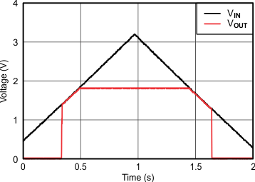
TLV74118P IOUT = 150 mA
Figure 20. VIN Power-Up and Power-Down
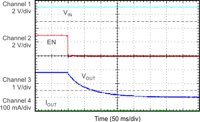
TLV741P G019_BVS195.gif
VIN = 3 V VOUT = 1.8 V CIN = COUT = 1 µF
TPS74118P No load
Figure 22. Shutdown Response With Enable