SNVSAV1A June 2017 – October 2017 TLV760
PRODUCTION DATA.
- 1 Features
- 2 Applications
- 3 Description
- 4 Revision History
- 5 Pin Configuration and Functions
- 6 Specifications
- 7 Detailed Description
- 8 Application and Implementation
- 9 Power Supply Recommendations
- 10Layout
- 11Device and Documentation Support
- 12Mechanical, Packaging, and Orderable Information
Package Options
Mechanical Data (Package|Pins)
- DBZ|3
Thermal pad, mechanical data (Package|Pins)
Orderable Information
10 Layout
10.1 Layout Guidelines
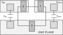
General guidelines for linear regulator designs are to place all circuit components on the same side of the circuit board and as near as practical to the respective TLV760 pin connections. Place ground return connections to the input and output capacitors, and to the TLV760 ground pin as close as possible to each other, connected by a wide, component-side, copper surface. The use of vias and long traces to create TLV760 circuit connections is strongly discouraged and negatively affects system performance.
Use a ground reference plane, either embedded in the PCB itself or located on the bottom side of the PCB opposite the components. This reference plane serves to assure accuracy of the output voltage and to shield noise; it behaves similarly to a thermal plane to spread heat from the linear regulator. In most applications, this ground plane is necessary to meet thermal requirements.
10.2 Layout Example
 Figure 25. Layout Guideline for TLV760