SNOSDA3F June   2020  – March 2023 TLV9020 , TLV9021 , TLV9022 , TLV9024 , TLV9030 , TLV9031 , TLV9032 , TLV9034

PRODMIX  

  1. Features
  2. Applications
  3. Description
  4. Revision History
  5. Pin Configuration and Functions
    1. 5.1 Pin Functions: TLV90x0 and TLV90x1 Single
    2.     Pin Functions: TLV90x2 Dual
    3.     Pin Functions: TLV90x4 Quad
  6. Specifications
    1. 6.1  Absolute Maximum Ratings
    2. 6.2  ESD Ratings
    3. 6.3  Recommended Operating Conditions
    4.     Thermal Information, TLV90x0,TLV90x1
    5. 6.4  Thermal Information, TLV90x2
    6. 6.5  Thermal Information, TLV90x4
    7. 6.6  Electrical Characteristics, TLV90x0,TLV90x1
    8. 6.7  Switching Characteristics, TLV90x0,TLV90x1
    9. 6.8  Electrical Characteristics, TLV90x2
    10. 6.9  Switching Characteristics, TLV90x2
    11. 6.10 Electrical Characteristics, TLV90x4
    12. 6.11 Switching Characteristics, TLV90x4
    13. 6.12 Typical Characteristics
  7. Detailed Description
    1. 7.1 Overview
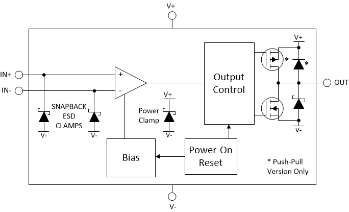
    2. 7.2 Functional Block Diagram
    3. 7.3 Feature Description
    4. 7.4 Device Functional Modes
      1. 7.4.1 Outputs
        1. 7.4.1.1 TLV9022 and TLV9024 Open Drain Output
        2. 7.4.1.2 TLV9032 and TLV9034 Push-Pull Output
      2. 7.4.2 Power-On Reset (POR)
      3. 7.4.3 Inputs
        1. 7.4.3.1 Rail to Rail Input
        2. 7.4.3.2 Fault Tolerant Inputs
        3. 7.4.3.3 Input Protection
      4. 7.4.4 ESD Protection
      5. 7.4.5 Unused Inputs
      6. 7.4.6 Hysteresis
  8. Application and Implementation
    1. 8.1 Application Information
      1. 8.1.1 Basic Comparator Definitions
        1. 8.1.1.1 Operation
        2. 8.1.1.2 Propagation Delay
        3. 8.1.1.3 Overdrive Voltage
      2. 8.1.2 Hysteresis
        1. 8.1.2.1 Inverting Comparator With Hysteresis
        2. 8.1.2.2 Non-Inverting Comparator With Hysteresis
        3. 8.1.2.3 Inverting and Non-Inverting Hysteresis Using Open-Drain Output
    2. 8.2 Typical Applications
      1. 8.2.1 Window Comparator
        1. 8.2.1.1 Design Requirements
        2. 8.2.1.2 Detailed Design Procedure
        3. 8.2.1.3 Application Curve
      2. 8.2.2 Square-Wave Oscillator
        1. 8.2.2.1 Design Requirements
        2. 8.2.2.2 Detailed Design Procedure
        3. 8.2.2.3 Application Curve
      3. 8.2.3 Adjustable Pulse Width Generator
      4. 8.2.4 Time Delay Generator
      5. 8.2.5 Logic Level Shifter
      6. 8.2.6 One-Shot Multivibrator
      7. 8.2.7 Bi-Stable Multivibrator
      8. 8.2.8 Zero Crossing Detector
      9. 8.2.9 Pulse Slicer
    3. 8.3 Power Supply Recommendations
  9. Layout
    1. 9.1 Layout Guidelines
    2. 9.2 Layout Example
  10. 10Device and Documentation Support
    1. 10.1 Documentation Support
      1. 10.1.1 Related Documentation
    2. 10.2 Receiving Notification of Documentation Updates
    3. 10.3 Support Resources
    4. 10.4 Trademarks
    5. 10.5 Electrostatic Discharge Caution
    6. 10.6 Glossary
  11. 11Mechanical, Packaging, and Orderable Information

Package Options

Mechanical Data (Package|Pins)
Thermal pad, mechanical data (Package|Pins)
Orderable Information

Functional Block Diagram

GUID-20200930-CA0I-LRN8-VXFX-LR9VXNNKXRKN-low.gif