SBOS941D February 2019 – August 2021 TLV9301 , TLV9302 , TLV9304
PRODUCTION DATA
- 1 Features
- 2 Applications
- 3 Description
- 4 Revision History
- 5 Pin Configuration and Functions
- 6 Specifications
- 7 Detailed Description
- 8 Application and Implementation
- 9 Power Supply Recommendations
- 10Layout
- 11Device and Documentation Support
- 12Mechanical, Packaging, and Orderable Information
Package Options
Mechanical Data (Package|Pins)
Thermal pad, mechanical data (Package|Pins)
- PW|14
Orderable Information
3 Description
The TLV930x family (TLV9301, TLV9302, and TLV9304) is a family of 40-V, cost-optimized operational amplifiers. These devices offer strong general-purpose DC and AC specifications, including rail-to-rail output, low offset (±0.5 mV, typ), low offset drift (±2 µV/°C, typ), and 1-MHz bandwidth.
Convenient features such as wide differential input-voltage range, high output current (±60 mA), and high slew rate (3 V/µs) make the TLV930x a robust operational amplifier for high-voltage, cost-sensitive applications.
The TLV930x family of op amps is available in standard packages and is specified from –40°C to 125°C.
| PART NUMBER(1) | PACKAGE | BODY SIZE (NOM) |
|---|---|---|
| TLV9301 | SOT-23 (5) | 2.90 mm × 1.60 mm |
| SC70 (5) | 2.00 mm × 1.25 mm | |
| TLV9302 | SOIC (8) | 4.90 mm × 3.91 mm |
| SOT-23-8 | 2.90 mm × 1.60 mm | |
| TSSOP (8) | 4.40 mm × 3.00 mm | |
| VSSOP (8) | 2.30 mm × 2.00 mm | |
| TLV9304 | SOIC (14) | 8.65 mm × 3.91 mm |
| TSSOP (14) | 5.00 mm × 4.40 mm |
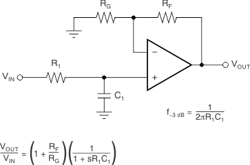
 TLV930x in a Single-Pole, Low-Pass Filter