SLVSGJ6 April 2022 TLVM13660
PRODUCTION DATA
- 1 Features
- 2 Applications
- 3 Description
- 4 Revision History
- 5 Device Comparison Table
- 6 Pin Configuration and Functions
- 7 Specifications
-
8 Detailed Description
- 8.1 Overview
- 8.2 Functional Block Diagram
- 8.3
Feature Description
- 8.3.1 Input Voltage Range (VIN1, VIN2)
- 8.3.2 Adjustable Output Voltage (FB)
- 8.3.3 Input Capacitors
- 8.3.4 Output Capacitors
- 8.3.5 Switching Frequency (RT)
- 8.3.6 Precision Enable and Input Voltage UVLO (EN)
- 8.3.7 Power Good Monitor (PG)
- 8.3.8 Adjustable Switch-Node Slew Rate (RBOOT, CBOOT)
- 8.3.9 Bias Supply Regulator (VCC, VLDOIN)
- 8.3.10 Overcurrent Protection (OCP)
- 8.3.11 Thermal Shutdown
- 8.4 Device Functional Modes
-
9 Applications and Implementation
- 9.1 Application Information
- 9.2
Typical Applications
- 9.2.1 Design 1 – High-Efficiency 6-A Synchronous Buck Regulator for Industrial Applications
- 9.2.2 Design 2 – Inverting Buck-Boost Regulator with Negative Output Voltage
- 10Power Supply Recommendations
- 11Layout
- 12Device and Documentation Support
- 13Mechanical, Packaging, and Orderable Information
Package Options
Mechanical Data (Package|Pins)
- RDL|20
Thermal pad, mechanical data (Package|Pins)
Orderable Information
10 Power Supply Recommendations
The TLVM13660 buck module is designed to operate over a wide input voltage range of 3 V to 36 V. The characteristics of the input supply must be compatible with the Absolute Maximum Ratings and Recommended Operating Conditions in this data sheet. In addition, the input supply must be capable of delivering the required input current to the loaded regulator circuit. Estimate the average input current with Equation 10.
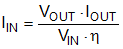
where
- η is the efficiency.
If the module is connected to an input supply through long wires or PCB traces with a large impedance, take special care to achieve stable performance. The parasitic inductance and resistance of the input cables can have an adverse affect on module operation. More specifically, the parasitic inductance in combination with the low-ESR ceramic input capacitors form an underdamped resonant circuit, possibly resulting in instability, voltage transients, or both, each time the input supply is cycled ON and OFF. The parasitic resistance causes the input voltage to dip during a load transient. If the module is operating close to the minimum input voltage, this dip can cause false UVLO triggering and a system reset.
The best way to solve such issues is to reduce the distance from the input supply to the module and use an electrolytic input capacitor in parallel with the ceramics. The moderate ESR of the electrolytic capacitor helps damp the input resonant circuit and reduce any overshoot or undershoot at the input. A capacitance in the range of 47 μF to 100 μF is usually sufficient to provide input parallel damping and helps hold the input voltage steady during large load transients. A typical ESR of 0.1 Ω to 0.4 Ω provides enough damping for most input circuit configurations.