SLYS016A June 2020 – October 2020 TMAG5124
PRODUCTION DATA
- 1
- 1 Features
- 2 Applications
- 3 Description
- 4 Revision History
- 5 Device Comparison Table
- 6 Pin Configuration and Functions
-
7 Specifications
- 7.1 Absolute Maximum Ratings
- 7.2 ESD Ratings
- 7.3 Recommended Operating Conditions
- 7.4 Thermal Information
- 7.5 Electrical Characteristics
- 7.6 Magnetic Characteristics
- 7.7 Typical Characteristics
- 8 Detailed Description
- 9 Application and Implementation
- 10Power Supply Recommendations
- 11Layout
- 12Device and Documentation Support
- 13Mechanical, Packaging, and Orderable Information
Package Options
Mechanical Data (Package|Pins)
- DBZ|3
Thermal pad, mechanical data (Package|Pins)
Orderable Information
3 Description
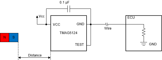
The TMAG5124 device is a high-precision Hall effect sensor that offers a 2-wire interface designed for industrial designs.
The TMAG5124 integrates a current source that switches between two levels depending on the value of the magnetic field applied to the part. While the high value is fixed, the low value can be selected from two ranges. This type of interface enables robust communication between sensor and controller, allow long distance transmissions, helps detect disconnections, and limits the number of wires to two.
The device is available in a 3-pin SOT-23 package. While 3 pins are available on the package, the device only requires the VCC and GND pin to operate. The current can be measured from either of those 2 pins, creating either a high-side or low-side configuration.
Different product variants enable selection of different levels of magnetic sensitivity to match application specific requirements.
The wide operating voltage range and reverse polarity protection of the TMAG5124 is designed for a variety of industrial applications.
| PART NUMBER | PACKAGE(1) | BODY SIZE (NOM) |
|---|---|---|
| TMAG5124 | SOT-23 (3) | 2.92 mm × 1.30 mm |
 Typical
Schematic