SBOS716D May   2015  – January 2020 TMP107

PRODUCTION DATA.  

  1. Features
  2. Applications
  3. Description
    1.     Device Images
      1.      Typical Application
  4. Revision History
  5. Pin Configuration and Functions
    1.     Pin Functions
  6. Specifications
    1. 6.1 Absolute Maximum Ratings
    2. 6.2 ESD Ratings
    3. 6.3 Recommended Operating Conditions
    4. 6.4 Thermal Information
    5. 6.5 Electrical Characteristics
    6. 6.6 Timing Requirements
    7. 6.7 Typical Characteristics
  7. Detailed Description
    1. 7.1 Overview
    2. 7.2 Functional Block Diagram
    3. 7.3 Feature Description
      1. 7.3.1 Digital Temperature Output
      2. 7.3.2 Temperature Limits and Alert
        1. 7.3.2.1 ALERT1, ALERT2, R1, and R2 Pins
      3. 7.3.3 SMAART Wire™ Communication Interface
        1. 7.3.3.1 Communication Protocol
          1. 7.3.3.1.1 Calibration Phase
          2. 7.3.3.1.2 Command and Address Phase
            1. 7.3.3.1.2.1 Global or Individual (G/nI) Bit
            2. 7.3.3.1.2.2 Read/Write (R/nW) Bit
            3. 7.3.3.1.2.3 Command or Address (C/nA) Bit:
          3. 7.3.3.1.3 Register Pointer Phase
          4. 7.3.3.1.4 Data Phase
        2. 7.3.3.2 SMAART Wire™ Operations
          1. 7.3.3.2.1 Command Operations
            1. 7.3.3.2.1.1 Address Initialize
            2. 7.3.3.2.1.2 Last Device Poll
            3. 7.3.3.2.1.3 Global Software Reset
          2. 7.3.3.2.2 Address Operations
            1. 7.3.3.2.2.1 Individual Write
            2. 7.3.3.2.2.2 Individual Read
            3. 7.3.3.2.2.3 Global Write
            4. 7.3.3.2.2.4 Global Read
    4. 7.4 Device Functional Modes
      1. 7.4.1 Continuous-Conversion Mode
      2. 7.4.2 Shutdown Mode
      3. 7.4.3 One-Shot Mode
    5. 7.5 Programming
      1. 7.5.1 EEPROM
      2. 7.5.2 EEPROM Operations
        1. 7.5.2.1 EEPROM Unlock
        2. 7.5.2.2 EEPROM Lock
        3. 7.5.2.3 EEPROM Programming
        4. 7.5.2.4 EEPROM Acquire or Read
    6. 7.6 Register Map
      1. 7.6.1 Temperature Register (address = 0h) [reset = 0h]
        1. Table 4. Temperature Register Field Descriptions
      2. 7.6.2 Configuration Register (address = 1h) [reset = A000h]
        1. Table 5. Configuration Register Field Descriptions
      3. 7.6.3 High Limit 1 Register (address = 2h) [reset = 7FFCh]
        1. Table 7. High Limit 1 Register Field Descriptions
      4. 7.6.4 Low Limit 1 Register (address = 3h) [reset = 8000h]
        1. Table 8. Low Limit 1 Register Field Descriptions
      5. 7.6.5 High Limit 2 Register (address = 4h) [reset = 7FFCh]
        1. Table 9. High Limit 2 Register Field Descriptions
      6. 7.6.6 Low Limit 2 Register (address = 5h) [reset = 8000h]
        1. Table 10. Low Limit 2 Register Field Descriptions
      7. 7.6.7 EEPROM n Register (where n = 1 to 8) (addresses = 6h to Dh) [reset = 0h]
        1. Table 11. EEPROM Register bits
      8. 7.6.8 Die ID Register (address = Fh) [reset = 1107h]
        1. Table 12. Die ID Register Field Descriptions
  8. Application and Implementation
    1. 8.1 Application Information
    2. 8.2 Typical Applications
      1. 8.2.1 Connecting Multiple Devices
        1. 8.2.1.1 Design Requirements
        2. 8.2.1.2 Detailed Design Procedure
          1. 8.2.1.2.1 Voltage Drop Effect
          2. 8.2.1.2.2 EEPROM Programming Current
          3. 8.2.1.2.3 Power Savings
          4. 8.2.1.2.4 Accuracy
          5. 8.2.1.2.5 Electromagnetic Interference (EMI)
        3. 8.2.1.3 Application Curves
      2. 8.2.2 Connecting ALERT1 and ALERT2 Pins
      3. 8.2.3 ALERT1 and ALERT2 Pins Used as General-Purpose Output (GPO)
  9. Power Supply Recommendations
  10. 10Layout
    1. 10.1 Layout Guidelines
    2. 10.2 Layout Example
  11. 11Device and Documentation Support
    1. 11.1 Documentation Support
      1. 11.1.1 Related Documentation
    2. 11.2 Receiving Notification of Documentation Updates
    3. 11.3 Community Resources
    4. 11.4 Trademarks
    5. 11.5 Electrostatic Discharge Caution
    6. 11.6 Glossary
  12. 12Mechanical, Packaging, and Orderable Information

Package Options

Mechanical Data (Package|Pins)
Thermal pad, mechanical data (Package|Pins)
Orderable Information

ALERT1 and ALERT2 Pins Used as General-Purpose Output (GPO)

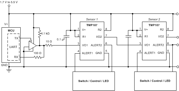
The TMP107 alert pins are also used as a GPO to control external switches or LEDs. This feature is useful in applications wherein the wiring between general-purpose output lines from the microcontroller or host to a control switch or LED can be eliminated by communicating through the I/O pins of TMP107. To configure the ALERTx pins as a GPO, program the high-limit register to the highest temperature (7FFCh) and the low-limit register to the lowest temperature (8000h). This programming disables the ALERTx pins from performing high- and low-limit temperature controls. The configuration register polarity bits (POL1 and POL2) are used to toggle the ALERTx pin output. The ALERTx pins are open-drain outputs; therefore, make sure the R1 and R2 pins are connected to the supply voltage, as shown in Figure 43.
TMP107 appdiagram4_sbos716.gifFigure 43. ALERT1 and ALERT2 Pins Used as General-Purpose Output