SBOS441I September 2009 – October 2019 TMP431 , TMP432
PRODUCTION DATA.
- 1 Features
- 2 Applications
- 3 Description
- 4 Revision History
- 5 Pin Configuration and Functions
- 6 Specifications
- 7 Parameter Measurement Information
-
8 Detailed Description
- 8.1 Overview
- 8.2 Functional Block Diagram
- 8.3 Feature Description
- 8.4 Device Functional Modes
- 8.5 Programming
- 8.6
Register Maps
- 8.6.1 Pointer Register
- 8.6.2 Temperature Registers
- 8.6.3 Limit Registers
- 8.6.4 Status Registers
- 8.6.5 Configuration Register 1
- 8.6.6 Configuration Register 2
- 8.6.7 Conversion Rate Register
- 8.6.8 Beta Compensation Configuration Register
- 8.6.9 η-Factor Correction Register
- 8.6.10 Software Reset
- 8.6.11 Consecutive Alert Register
- 8.6.12 Therm Hysteresis Register
- 8.6.13 Identification Registers
- 8.6.14 Open Status Register
- 8.6.15 Channel Mask Register
- 8.6.16 High Limit Status Register
- 8.6.17 Low Limit Status Register
- 8.6.18 THERM Limit Status Register
- 9 Application and Implementation
- 10Power Supply Recommendations
- 11Layout
- 12Device and Documentation Support
- 13Mechanical, Packaging, and Orderable Information
Package Options
Mechanical Data (Package|Pins)
- DGS|10
Thermal pad, mechanical data (Package|Pins)
Orderable Information
8.5.10 SMBus Alert Function
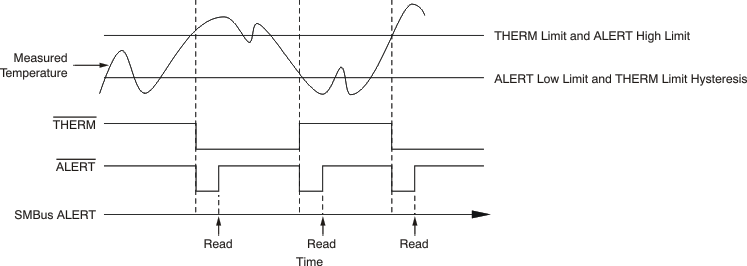
The TMP43x support the SMBus Alert function. When pin 6 (for the TMP431) or pin 8 (for the TMP432) is configured as an alert output, the ALERT pin of the TMP43x can be connected as an SMBus Alert signal. When a master detects an alert condition on the ALERT line, the master sends an SMBus Alert command (00011001) on the bus. If the ALERT pin of the TMP43x is active, the devices acknowledge the SMBus Alert command and respond by returning the slave address on the SDA line and release the SMBus alert line after the acknowledgement of their address. The eighth bit (LSB) of the slave address byte indicates whether the temperature exceeding one of the temperature high limit settings or falling below one of the temperature low limit settings caused the alert condition. This bit is high if the temperature is greater than or equal to one of the temperature high limit settings; this bit is low if the temperature is less than one of the temperature low limit settings. After acknowledging the slave address, the device disengages its ALERT pulldown. The TMP43x disengages the ALERT pulldown by setting the ALERT Mask Bit in the Configuration Register after sending out its address in response to an ARA and releases the ALERT output pin. This command will not clear the previous alert. Once the ALERT Mask bit is activated, the ALERT output pin will be disabled until enabled by software. In order to enable the ALERT, the master must read the ALERT Status Register during the interrupt service routine, and then reset the ALERT Mask bit in the Configuration Register to 0 at the end of the interrupt service. routine. See Figure 18 for details of this sequence.
 Figure 18. SMBus Alert Timing Diagram
 If multiple devices on the bus respond to the SMBus Alert command, arbitration during the slave address portion of the SMBus Alert command determines which device clears its alert status. If the TMP43x win the arbitration, the ALERT pin becomes inactive at the completion of the SMBus Alert command. If the TMP43x lose the arbitration, the ALERT pin remains active.