SBOS686A June 2013 – December 2014 TMP451
PRODUCTION DATA.
- 1 Features
- 2 Applications
- 3 Description
- 4 Revision History
- 5 Pin Configuration and Functions
- 6 Specifications
-
7 Detailed Description
- 7.1 Overview
- 7.2 Functional Block Diagram
- 7.3 Feature Description
- 7.4 Device Functional Modes
- 7.5 Programming
- 7.6
Register Map
- 7.6.1
Register Information
- 7.6.1.1 Pointer Register
- 7.6.1.2 Temperature Registers
- 7.6.1.3 Local Temperature High Byte Register (offset: Read = 00h; Write = N/A) [reset = 00h]
- 7.6.1.4 Remote Temperature High Byte Register (offset: Read = 01h; Write = N/A) [reset = 00h]
- 7.6.1.5 Status Register (offset: Read = 02h; Write = N/A) [reset = N/A]
- 7.6.1.6 Configuration Register (offset: Read = 03h; Write = 09h) [reset = 00h]
- 7.6.1.7 Conversion Rate Register (offset: Read = 04h; Write = 0Ah) [reset = 08h]
- 7.6.1.8 Local Temperature High Limit Register (offset: Read = 05h; Write = 0Bh) [reset = 55h]
- 7.6.1.9 Local Temperature Low Limit Register (offset: Read = 06h; Write = 0Ch) [reset = 00h]
- 7.6.1.10 Remote Temperature High Limit High Byte Register (offset: Read = 07h; Write = 0Dh) [reset = 55h]
- 7.6.1.11 Remote Temperature Low Limit High Byte Register (offset: Read = 08h; Write = 0Eh) [reset = 00h]
- 7.6.1.12 One-shot Start Register (offset: Read = N/A; Write = 0Fh) [reset = N/A]
- 7.6.1.13 Remote Temperature Low Byte Register (offset: Read = 10h; Write = N/A) [reset = 00h]
- 7.6.1.14 Remote Temperature Offset High Byte Register (offset: Read = 11h; Write = 11h) [reset = 00h]
- 7.6.1.15 Remote Temperature Offset Low Byte Register (offset: Read = 12h; Write = 12h) [reset = 00h]
- 7.6.1.16 Remote Temperature High Limit Low Byte Register (offset: Read = 13h; Write = 13h) [reset = 00h]
- 7.6.1.17 Remote Temperature Low Limit Low Byte Register (offset: Read = 14h; Write = 14h) [reset = 00h]
- 7.6.1.18 Local Temperature Low Byte Register (offset: Read = 15h; Write = N/A) [reset = 00h]
- 7.6.1.19 Remote Temperature THERM Limit Register (offset: Read = 19h; Write = 19h) [reset = 6C]
- 7.6.1.20 Local Temperature THERM Limit Register (offset: Read = 20h; Write = 20h) [reset = 55]
- 7.6.1.21 THERM Hysteresis Register (offset: Read = 21h; Write = 21h) [reset = 0Ah]
- 7.6.1.22 Consecutive ALERT Register (offset: Read = 22h; Write = 22h) [reset = 01h]
- 7.6.1.23 η-Factor Correction Register (offset: Read = 23h; Write = 23h) [reset = 00h]
- 7.6.1.24 Digital Filter Control Register (offset: Read = 24h; Write = 24h) [reset = 00h]
- 7.6.1.25 Manufacturer ID Register (offset: Read = FEh; Write = N/A) [reset = 55]
- 7.6.1
Register Information
- 8 Application and Implementation
- 9 Power Supply Recommendations
- 10Layout
- 11Device and Documentation Support
- 12Mechanical, Packaging, and Orderable Information
Package Options
Mechanical Data (Package|Pins)
- DQF|8
Thermal pad, mechanical data (Package|Pins)
- DQF|8
Orderable Information
7 Detailed Description
7.1 Overview
The TMP451 device is a digital temperature sensor that combines a local temperature measurement channel and a remote-junction temperature measurement channel in a single DFN-8 package. The device is two-wire- and SMBus-interface compatible, and is specified over a temperature range of –40°C to 125°C. The TMP451 device also contains multiple registers for programming and holding configuration settings, temperature limits, and temperature measurement results.
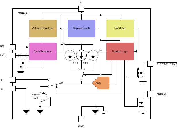
7.2 Functional Block Diagram
7.3 Feature Description
7.3.1 Temperature Measurement Data
The local and remote temperature sensors have a resolution of 12 bits (0.0625°C). Temperature data that result from conversions within the default measurement range are represented in binary form, as shown in the STANDARD BINARY column of Table 1. Any temperature below 0°C results in a data value of 0 (00h). Likewise, temperatures above 127°C result in a value of 127 (7Fh). The device can be set to measure over an extended temperature range by changing bit 2 (RANGE) of configuration register from low to high. The change in measurement range and data format from standard binary to extended binary occurs at the next temperature conversion. For data captured in the extended temperature range configuration, an offset of 64 (40h) is added to the standard binary value, as shown in the EXTENDED BINARY column of Table 1. This configuration allows measurement of temperatures as low as –64°C, and as high as 191°C; however, most temperature-sensing diodes only measure with the range of –55°C to 150°C. Additionally, the TMP451 device is specified only for ambient temperatures ranging from –40°C to 125°C; parameters in the Absolute Maximum Ratings table must be observed.
Table 1. Temperature Data Format (Local and Remote Temperature High Bytes)
| TEMPERATURE (°C) |
LOCAL AND REMOTE TEMPERATURE REGISTER HIGH BYTE VALUE (1°C RESOLUTION) |
|||
|---|---|---|---|---|
| STANDARD BINARY(1) | EXTENDED BINARY(2) | |||
| BINARY | HEX | BINARY | HEX | |
| –64 | 0000 0000 | 00 | 0000 0000 | 00 |
| –50 | 0000 0000 | 00 | 0000 1110 | 0E |
| –25 | 0000 0000 | 00 | 0010 0111 | 27 |
| 0 | 0000 0000 | 00 | 0100 0000 | 40 |
| 1 | 0000 0001 | 01 | 0100 0001 | 41 |
| 5 | 0000 0101 | 05 | 0100 0101 | 45 |
| 10 | 0000 1010 | 0A | 0100 1010 | 4A |
| 25 | 0001 1001 | 19 | 0101 1001 | 59 |
| 50 | 0011 0010 | 32 | 0111 0010 | 72 |
| 75 | 0100 1011 | 4B | 1000 1011 | 8B |
| 100 | 0110 0100 | 64 | 1010 0100 | A4 |
| 125 | 0111 1101 | 7D | 1011 1101 | BD |
| 127 | 0111 1111 | 7F | 1011 1111 | BF |
| 150 | 0111 1111 | 7F | 1101 0110 | D6 |
| 175 | 0111 1111 | 7F | 1110 1111 | EF |
| 191 | 0111 1111 | 7F | 1111 1111 | FF |
Both local and remote temperature data use two bytes for data storage. The high byte stores the temperature with 1°C resolution. The second or low byte stores the decimal fraction value of the temperature and allows a higher measurement resolution, as shown in Table 2. The measurement resolution for both the local and the remote channels is 0.0625°C.
Table 2. Decimal Fraction Temperature Data Format (Local and Remote Temperature Low Bytes)
| TEMP (°C) |
TEMPERATURE REGISTER LOW BYTE VALUE (0.0625°C RESOLUTION)(1) |
|
|---|---|---|
| STANDARD AND EXTENDED BINARY | HEX | |
| 0 | 0000 0000 | 00 |
| 0.0625 | 0001 0000 | 10 |
| 0.1250 | 0010 0000 | 20 |
| 0.1875 | 0011 0000 | 30 |
| 0.2500 | 0100 0000 | 40 |
| 0.3125 | 0101 0000 | 50 |
| 0.3750 | 0110 0000 | 60 |
| 0.4375 | 0111 0000 | 70 |
| 0.5000 | 1000 0000 | 80 |
| 0.5625 | 1001 0000 | 90 |
| 0.6250 | 1010 0000 | A0 |
| 0.6875 | 1011 0000 | B0 |
| 0.7500 | 1100 0000 | C0 |
| 0.8125 | 1101 0000 | D0 |
| 0.8750 | 1110 0000 | E0 |
| 0.9385 | 1111 0000 | F0 |
7.3.1.1 Standard Binary-to-Decimal Temperature Data Calculation Example
High-byte conversion (for example, 0111 0011):
Convert the right-justified binary high byte to hexadecimal.
From hexadecimal, multiply the first number by 160 = 1 and the second number by 161 = 16.
The sum equals the decimal equivalent.
0111 0011b → 73h → (3 × 160) + (7 × 161) = 115
Low-byte conversion (for example, 0111 0000):
To convert the left-justified binary low-byte to decimal, use bits 7 through 4 and ignore bits 3 through 0 because they do not affect the value of the number.
0111b → (0 × 1/2)1 + (1 × 1/2)2 + (1 × 1/2)3 + (1 × 1/2)4 = 0.4375
7.3.1.2 Standard Decimal-to-Binary Temperature Data Calculation Example
For positive temperatures (for example, 20°C):
(20°C) / (1°C/count) = 20 → 14h → 0001 0100
Convert the number to binary code with 8-bit, right-justified format, and MSB = 0 to denote a positive sign.
20°C is stored as 0001 0100 → 14h.
For negative temperatures (for example, –20°C):
(|–20|) / (1°C/count) = 20 → 14h → 0001 0100
Generate the two's complement of a negative number by complementing the absolute value binary number and adding 1.
–20°C is stored as 1110 1100 → ECh.
7.3.2 Series Resistance Cancellation
Series resistance cancellation automatically eliminates the temperature error caused by the resistance of the routing to the remote transistor or by the resistors of the optional external low-pass filter. A total of up to 1 kΩ of series resistance can be cancelled by the TMP451 device, eliminating the need for additional characterization and temperature offset correction. See Figure 5 for details on the effects of series resistance on sensed remote temperature error.
7.3.3 Differential Input Capacitance
The TMP451 device tolerates differential input capacitance of up to 1000 pF with minimal change in temperature error. The effect of capacitance on sensed remote temperature error is shown in Figure 6.
7.3.4 Filtering
Remote junction temperature sensors are usually implemented in a noisy environment. Noise is most often created by fast digital signals, and it can corrupt measurements. The TMP451 device has a built-in, 65-kHz filter on the inputs of D+ and D– to minimize the effects of noise. However, a bypass capacitor placed differentially across the inputs of the remote temperature sensor is recommended to make the application more robust against unwanted coupled signals. For this capacitor, select a value of between 100 pF and 1 nF. Some applications attain better overall accuracy with additional series resistance; however, this increased accuracy is application-specific. When series resistance is added, the total value should not be greater than 1 kΩ. If filtering is required, suggested component values are 100 pF and 50 Ω on each input; exact values are application-specific.
Additionally, a digital filter is available for the remote temperature measurements to further reduce the effect of noise. This filter is programmable and has two levels when enabled. Level 1 performs a moving average of four consecutive samples. Level 2 performs a moving average of eight consecutive samples. The value stored in the remote temperature result register is the output of the digital filter, and the ALERT and THERM limits are compared to it. This provides additional immunity to noise and spikes on the ALERT and THERM outputs. The filter responses are shown in Figure 12. The filter can be enabled or disabled by programming the desired levels in the digital filter register. The digital filter is disabled by default and on POR.
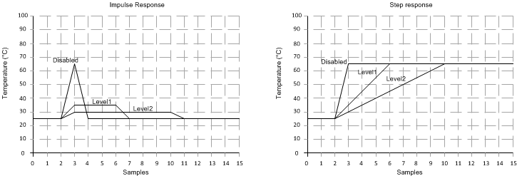 Figure 12. Filter Response to Impulse and Step Inputs
7.3.5 Sensor Fault
The TMP451 device can sense a fault at the D+ input resulting from incorrect diode connection. The TMP451 device can also sense an open circuit. Short-circuit conditions return a value of –64°C. The detection circuitry consists of a voltage comparator that trips when the voltage at D+ exceeds (V+) – 0.3 V (typical). The comparator output is continuously checked during a conversion. If a fault is detected, then OPEN (bit 2) in the status register is set to 1.
When not using the remote sensor with the TMP451 device, the D+ and D– inputs must be connected together to prevent meaningless fault warnings.
7.3.6 ALERT and THERM Functions
The operation of the ALERT (pin 6) and THERM (pin 4) interrupts is shown in Figure 13. The operation of the THERM (pin 4) and THERM2 (pin 6) interrupts is shown in Figure 14.
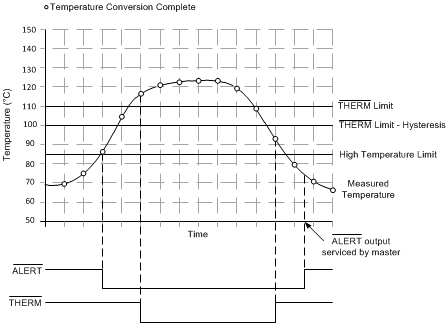 Figure 13. ALERT and THERM Interrupt Operation
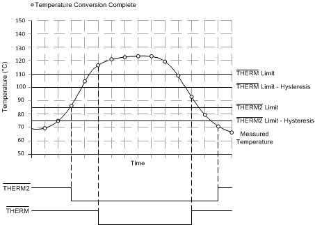 Figure 14. THERM and THERM2 Interrupt Operation
The hysteresis value is stored in the THERM hysteresis register. The value of the CONAL[2:0] bits in the consecutive ALERT register determines the number of limit violations before the ALERT pin is tripped. The default value is 000b and corresponds to one violation, 001b programs two consecutive violations, 011b programs three consecutive violations, and 111b programs four consecutive violations. This provides additional filtering for the ALERT pin state.
7.4 Device Functional Modes
7.4.1 Shutdown Mode (SD)
The TMP451 shutdown mode enables the user to save maximum power by shutting down all device circuitry other than the serial interface, reducing current consumption to typically less than 3 μA; see Figure 11. Shutdown mode is enabled when the SD bit (bit 6) of the configuration register is high; the device shuts down after the current conversion is finished. When the SD bit is low, the device maintains a continuous-conversion state.
7.4.2 One-shot Mode
When the TMP451 device is in shutdown mode (SD = 1 in the configuration register), a single conversion is started by writing any value to the one-shot start register, pointer address 0Fh. This write operation starts one conversion and comparison cycle on both the local and the remote sensors. The TMP451 device returns to shutdown mode when the cycle completes. The value of the data sent in the write command is irrelevant and is not stored by the TMP451 device.
7.5 Programming
7.5.1 Serial Interface
The TMP451 device operates only as a slave device on either the two-wire bus or the SMBus. Connections to either bus are made using the open-drain I/O lines, SDA and SCL. The SDA and SCL pins feature integrated spike suppression filters and Schmitt triggers to minimize the effects of input spikes and bus noise. The TMP451 device supports the transmission protocol for fast (1 kHz to 400 kHz) and high-speed (1 kHz to 2.5 MHz) modes. All data bytes are transmitted MSB first.
7.5.1.1 Bus Overview
The TMP451 device is SMBus interface compatible. In SMBus protocol, the device that initiates the transfer is called a master, and the devices controlled by the master are slaves. The bus must be controlled by a master device that generates the serial clock (SCL), controls the bus access, and generates the START and STOP conditions.
To address a specific device, a START condition is initiated. A START condition is indicated by pulling the data line (SDA) from a high-to-low logic level while SCL is high. All slaves on the bus shift in the slave address byte, with the last bit indicating whether a read or write operation is intended. During the ninth clock pulse, the slave being addressed responds to the master by generating an acknowledge bit and pulling SDA low.
Data transfer is then initiated and sent over eight clock pulses followed by an acknowledge bit. During data transfer SDA must remain stable while SCL is high, because any change in SDA while SCL is high is interpreted as a control signal.
After all data have been transferred, the master generates a STOP condition. A STOP condition is indicated by pulling SDA from low to high, while SCL is high.
7.5.1.2 Bus Definitions
The TMP451 device is two-wire and SMBus-compatible. Figure 15 and Figure 16 show the timing for various operations on the TMP451 device. The bus definitions are as follows:
-
Acknowledge:Each receiving device, when addressed, is obliged to generate an acknowledge bit. A device that acknowledges must pull down the SDA line during the acknowledge clock pulse in such a way that the SDA line is stable low during the high period of the acknowledge clock pulse. Take setup and hold times into account. On a master receive, data transfer termination can be signaled by the master generating a not-acknowledge on the last byte that has been transmitted by the slave.
-
Bus Idle: Both SDA and SCL lines remain high.
-
Data Transfer:The number of data bytes transferred between a START and a STOP condition is not limited and is determined by the master device. The receiver acknowledges data transfer.
-
Start Data Transfer:A change in the state of the SDA line, from high to low, while the SCL line is high, defines a start condition. Each data transfer initiates with a START condition.
-
Stop Data Transfer: A change in the state of the SDA line from low to high while the SCL line is high defines a STOP condition. Each data transfer terminates with a repeated START or STOP condition.
7.5.1.3 Serial Bus Address
To communicate with the TMP451 device, the master must first address slave devices using a slave address byte. The slave address byte consists of seven address bits, and a direction bit indicating the intent of executing a read or write operation. The TMP451 device has a device address of 4Ch (1001 100b). Additional factory-programmed device addresses are available upon request.
7.5.1.4 Read and Write Operations
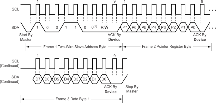
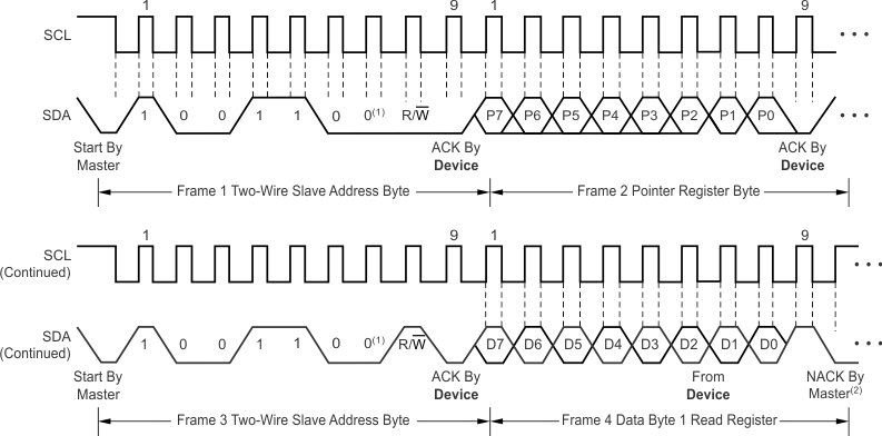
Accessing a particular register on the TMP451 device is accomplished by writing the appropriate value to the pointer register. The value for the pointer register is the first byte transferred after the slave address byte with the R/W bit low. Every write operation to the TMP451 device requires a value for the pointer register (see Figure 15).
When reading from the TMP451 device the last value stored in the pointer register by a write operation is used to determine which register is read by a read operation. To change which register is read for a read operation, a new value must be written to the pointer register. This transaction is accomplished by issuing a slave address byte with the R/W bit low, followed by the pointer register byte; no additional data are required. The master can then generate a START condition and send the slave address byte with the R/W bit high to initiate the read command; see Figure 16 for details of this sequence.
If repeated reads from the same register are desired, it is not necessary to continually send the pointer register bytes, because the TMP451 device retains the pointer register value until it is changed by the next write operation. The register bytes are sent MSB first, followed by the LSB.
Read operations should be terminated by issuing a not-acknowledge command at the end of the last byte to be read. For single-byte operation, the master must leave the SDA line high during the acknowledge time of the first byte that is read from the slave.
7.5.1.5 Time-out Function
If the SMBus time-out function is enabled, the TMP451 device resets the serial interface if either SCL or SDA are held low for 25 ms (typical) between a START and STOP condition. If the TMP451 device is holding the bus low, the device releases the bus and waits for a START condition. To avoid activating the time-out function, maintaining a communication speed of at least 1 kHz for the SCL operating frequency is necessary. The SMBTO bit (bit 7) of the consecutive ALERT register controls the time-out enable. Setting the SMBTO bit to a value of 0 (default) disables the time-out. Setting the SMBTO bit to a value of 1 enables the function.
7.5.1.6 High-speed Mode
For the two-wire bus to operate at frequencies above 1 MHz, the master device must issue a high-speed mode (Hs-mode) master code (0000 1xxx) as the first byte after a START condition to switch the bus to high-speed operation. The TMP451 device does not acknowledge this byte, but switches the input filters on SDA and SCL and the output filter on SDA to operate in Hs-mode, allowing transfers at up to 2.5 MHz. After the Hs-mode master code has been issued, the master transmits a two-wire slave address to initiate a data transfer operation. The bus continues to operate in Hs-mode until a STOP condition occurs on the bus. Upon receiving the STOP condition, the TMP451 device switches the input and output filters back to fast mode operation.
7.5.1.7 General Call Reset
The TMP451 device supports reset using the two-wire general call address 00h (0000 0000b). The TMP451 device acknowledges the general call address and responds to the second byte. If the second byte is 06h (0000 0110b), the TMP451 device executes a software reset. This software reset restores the power-on reset state to all TMP451 registers, and it aborts any conversion in progress. The TMP451 device takes no action in response to other values in the second byte.
7.6 Register Map
Table 3. Register Map
| POINTER READ (HEX) | POINTER WRITE (HEX) | POR (HEX) | BIT DESCRIPTION | REGISTER DESCRIPTION | |||||||
|---|---|---|---|---|---|---|---|---|---|---|---|
| 7 | 6 | 5 | 4 | 3 | 2 | 1 | 0 | ||||
| 00 | N/A | 00 | LT11 | LT10 | LT9 | LT8 | LT7 | LT6 | LT5 | LT4 | Local temperature (high byte) |
| 01 | N/A | 00 | RT11 | RT10 | RT9 | RT8 | RT7 | RT6 | RT5 | RT4 | Remote temperature (high byte) |
| 02 | N/A | N/A | BUSY | LHIGH | LLOW | RHIGH | RLOW | OPEN | RTHRM | LTHRM | Status register |
| 03 | 09 | 00 | MASK1 | SD | ALERT/ THERM2 |
0 | 0 | RANGE | 0 | 0 | Configuration register |
| 04 | 0A | 08 | 0 | 0 | 0 | 0 | CR3 | CR2 | CR1 | CR0 | Conversion rate register |
| 05 | 0B | 55 | LTHL11 | LTHL10 | LTHL9 | LTHL8 | LTHL7 | LTHL6 | LTHL5 | LTHL4 | Local temperature high limit |
| 06 | 0C | 00 | LTLL11 | LTLL10 | LTLL9 | LTLL8 | LTLL7 | LTLL6 | LTLL5 | LTLL4 | Local temperature low limit |
| 07 | 0D | 55 | RTHL11 | RTHL10 | RTHL9 | RTHL8 | RTHL7 | RTHL6 | RTHL5 | RTHL4 | Remote temperature high limit (high byte) |
| 08 | 0E | 00 | RTLL11 | RTLL10 | RTLL9 | RTLL8 | RTLL7 | RTLL6 | RTLL5 | RTLL4 | Remote temperature low limit (high byte) |
| N/A | 0F | N/A | X | X | X | X | X | X | X | X | One-shot start Table 14 |
| 10 | N/A | 00 | RT3 | RT2 | RT1 | RT0 | 0 | 0 | 0 | 0 | Remote temperature (low byte) |
| 11 | 11 | 00 | RTOS11 | RTOS10 | RTOS9 | RTOS8 | RTOS7 | RTOS6 | RTOS5 | RTOS4 | Remote temperature offset (high byte) |
| 12 | 12 | 00 | RTOS3 | RTOS2 | RTOS1 | RTOS0 | 0 | 0 | 0 | 0 | Remote temperature offset (low byte) |
| 13 | 13 | 00 | RTHL3 | RTHL2 | RTHL1 | RTHL0 | 0 | 0 | 0 | 0 | Remote temperature high limit (low byte) |
| 14 | 14 | 00 | RTLL3 | RTLL2 | RTLL1 | RTLL0 | 0 | 0 | 0 | 0 | Remote temperature low limit (low byte) |
| 15 | N/A | 00 | LT3 | LT2 | LT1 | LT0 | 0 | 0 | 0 | 0 | Local temperature (low byte) |
| 19 | 19 | 6C | RTH11 | RTH10 | RTH9 | RTH8 | RTH7 | RTH6 | RTH5 | RTH4 | Remote temperature THERM limit |
| 20 | 20 | 55 | LTH11 | LTH10 | LTH9 | LTH8 | LTH7 | LTH6 | LTH5 | LTH4 | Local temperature THERM limit |
| 21 | 21 | 0A | HYS11 | HYS10 | HYS9 | HYS8 | HYS7 | HYS6 | HYS5 | HYS4 | THERM hysteresis |
| 22 | 22 | 01 | SMBTO | 0 | 0 | 0 | CONAL2 | CONAL1 | CONAL0 | 1 | Consecutive ALERT |
| 23 | 23 | 00 | NC7 | NC6 | NC5 | NC4 | NC3 | NC2 | NC1 | NC0 | η-factor correction |
| 24 | 24 | 00 | 0 | 0 | 0 | 0 | 0 | 0 | DF1 | DF0 | Digital filter control |
| FE | N/A | 55 | 0 | 1 | 0 | 1 | 0 | 1 | 0 | 1 | Manufacturer ID |
7.6.1 Register Information
The TMP451 device contains multiple registers for holding configuration information, temperature measurement results, and status information. These registers are described in Figure 17 and Table 3.
7.6.1.1 Pointer Register
Figure 17 shows the internal register structure of the TMP451 device. The 8-bit pointer register is used to address a given data register. The pointer register identifies which of the data registers should respond to a read or write command on the two-wire bus. This register is set with every write command. A write command must be issued to set the proper value in the pointer register before executing a read command. Table 3 describes the pointer register and the internal structure of the TMP451 registers. The power-on reset (POR) value of the pointer register is 00h (0000 0000b).
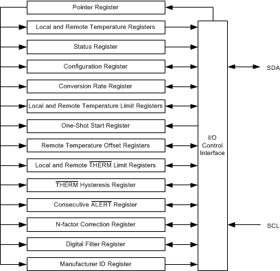 Figure 17. Internal Register Structure
7.6.1.2 Temperature Registers
The TMP451 device has multiple 8-bit registers that hold temperature measurement results. The eight most significant bits (MSBs) of the local temperature sensor result are stored in register 00h, while the four least significant bits (LSBs) are stored in register 15h (the four MSBs of register 15h). The eight MSBs of the remote temperature sensor result are stored in register 01h, and the four LSBs are stored in register 10h (the four MSBs of register 10h). The four LSBs of both the local sensor and the remote sensor indicate the temperature value after the decimal point (for example, if the temperature result is 10.0625˚C, the high byte is 0000 1010 and the low byte is 0001 0000). These registers are read-only and are updated by the ADC each time a temperature measurement.
When the full temperature value is needed, reading the MSB value first causes the LSB value to be locked (the ADC does not write to it) until it is read. The same thing happens upon reading the LSB value first (the MSB value is locked until it is read). This mechanism assures that both bytes of the read operation are from the same ADC conversion. This assurance remains valid only until another register is read. For proper operation, read the high byte of the temperature result first. Read the low byte register in the next read command; if the LSBs are not needed, the register may be left unread. The power-on reset value of all temperature registers is 00h.
7.6.1.3 Local Temperature High Byte Register (offset: Read = 00h; Write = N/A) [reset = 00h]
| 7 | 6 | 5 | 4 | 3 | 2 | 1 | 0 |
| LT11 | LT10 | LT9 | LT8 | LT7 | LT6 | LT5 | LT4 |
| R-0 | R-0 | R-0 | R-0 | R-0 | R-0 | R-0 | R-0 |
| LEGEND: R/W = Read/Write; R = Read only; -n = value after reset |
Table 4. Local Temperature High Byte Register Field Descriptions
| Bit | Field | Type | Reset | Description |
|---|---|---|---|---|
| 7 - 0 | LT11 - LT4 | R | 0h |
Local temperature high byte. The resolution of the LSB in this register is 1°C. This register is read-only and is updated by the ADC each time a temperature measurement is completed. When the full temperature value is needed, reading the high byte register first causes the low byte register value to be locked (the ADC does not write to it) until it is read. The same thing happens upon reading the low byte register value first (the high byte register value is locked until it is read). This mechanism assures that both bytes of the read operation are from the same ADC conversion. This assurance remains valid only until another register is read. For proper operation, read the high byte of the temperature result first. Read the low byte register in the next read command; if the low byte is not needed, the register may be left unread. |
7.6.1.4 Remote Temperature High Byte Register (offset: Read = 01h; Write = N/A) [reset = 00h]
| 7 | 6 | 5 | 4 | 3 | 2 | 1 | 0 |
| RT11 | RT10 | RT9 | RT8 | RT7 | RT6 | RT5 | RT4 |
| R-0h | R-0h | R-0h | R-0h | R-0h | R-0h | R-0h | R-0h |
| LEGEND: R/W = Read/Write; R = Read only; -n = value after reset |
Table 5. Remote Temperature High Byte Register Field Descriptions
| Bit | Field | Type | Reset | Description |
|---|---|---|---|---|
| 7 - 0 | RT11 - RT4 | R | 0h | Remote temperature high byte. The resolution of the LSB in this register is 1 °C. This register is read-only and is updated by the ADC each time a temperature measurement is completed. When the full temperature value is needed, reading the high byte register first causes the low byte register value to be locked (the ADC does not write to it) until it is read. The same thing happens upon reading the low byte register value first (the high byte register value is locked until it is read). This mechanism assures that both bytes of the read operation are from the same ADC conversion. This assurance remains valid only until another register is read. For proper operation, read the high byte of the temperature result first. Read the low byte register in the next read command; if the low byte is not needed, the register may be left unread. |
7.6.1.5 Status Register (offset: Read = 02h; Write = N/A) [reset = N/A]
| 7 | 6 | 5 | 4 | 3 | 2 | 1 | 0 |
| BUSY | LHIGH | LLOW | RHIGH | RLOW | OPEN | RTHRM | LTHRM |
| R | R | R | R | R | R | R | R |
| LEGEND: R/W = Read/Write; R = Read only; -n = value after reset |
Table 6. Status Register Field Descriptions
| Bit | Field | Type | Reset | Description |
|---|---|---|---|---|
| 7 | BUSY | R | N/A |
ADC status indicator 1 = ADC is converting. 0 = ADC is not converting. |
| 6 | LHIGH | R | N/A | Local temperature high limit status indicator(1)
1 = Local temperature value exceeds the Local Temperature High Limit Register value. This bit is cleared upon reading the Status Register providing that the condition causing the over temperature result is no longer present. 0 = Local temperature value does not exceed the Local Temperature High Limit Register value. |
| 5 | LLOW | R | N/A | Local temperature low limit status indicator(1)
1 = Local temperature value is below the Local Temperature Low Limit Register value. This bit is cleared upon reading the Status Register providing that the condition causing the under temperature result is no longer present. 0 = Local temperature value is not below the Local Temperature Low Limit Register value. |
| 4 | RHIGH | R | N/A | Remote temperature high limit status indicator(1)
1 = Remote temperature value exceeds the Remote Temperature High Limit Register value. This bit is cleared upon reading the Status Register providing that the condition causing the over temperature result is no longer present. 0 = Remote temperature value does not exceed the Remote Temperature High Limit Register value. |
| 3 | RLOW | R | N/A | Remote temperature low limit status indicator(1)
1 = Remote temperature value is below the Remote Temperature Low Limit Register value. This bit is cleared upon reading the Status Register providing that the condition causing the under temperature result is no longer present. 0 = Remote temperature value is not below the Remote Temperature Low Limit Register value. |
| 2 | OPEN | R | N/A | Remote junction open circuit detection(1)
1 = The remote junction is an open circuit. This bit is cleared upon reading the Status Register providing that the condition causing the open circuit is no longer present. 0 = The remote junction is not an open circuit. |
| 1 | RTHRM | R | N/A |
Remote THERM limit status indicator 1 = Remote THERM limit is tripped. This bit is cleared upon reading the Status Register providing that the condition causing the over temperature result is no longer present. 0 = Remote THERM limit is not tripped. |
| 0 | LTHRM | R | N/A |
Local THERM limit status indicator 1 = Local THERM limit is tripped. This bit is cleared upon reading the Status Register providing that the condition causing the over temperature result is no longer present. 0 = Local THERM limit is not tripped. |
The status register reports the state of the temperature ADC, the temperature limit comparators, and the connection to the remote sensor. Table 6 lists the status register bits. The status register is read-only, and is read by accessing pointer address 02h.
The LHIGH and LLOW bits indicate a local sensor overtemperature or undertemperature event, respectively. The RHIGH and RLOW bits indicate a remote sensor overtemperature or undertemperature event, respectively. The OPEN bit indicates an open-circuit condition on the remote sensor. When pin 6 is configured as the ALERT output, the five flags are NORed together. If any of the five flags are high, the ALERT interrupt latch is set and the ALERT output goes low. Reading the status register clears the five flags, provided that the condition that caused the setting of the flags is not present anymore (that is, the value of the corresponding result register is within the limits, or the remote sensor is connected properly and functional). The ALERT interrupt latch (and the ALERT pin correspondingly) is not reset by reading the status register. The reset is done by the master reading the temperature sensor device address to service the interrupt, and only if the flags have been reset and the condition that caused them to be set is not present.
The RTHRM and LTHRM flags are set when the corresponding temperature exceeds the programmed THERM limit. They are reset automatically when the temperature returns to within the limits. The THERM output goes low in the case of overtemperature on either the local or the remote channel, and goes high as soon as the measurements are within the limits again. The THERM hysteresis register (21h) allows hysteresis to be added so that the flag resets and the output goes high when the temperature returns to or goes below the limit value minus the hysteresis value.
When pin 6 is configured as THERM2, only the high limits matter. The LHIGH and RHIGH flags are set if the respective temperatures exceed the limit values, and the pin goes low to indicate the event. The LLOW and RLOW flags have no effect on THERM2, and the output behaves the same way when configured as THERM.
7.6.1.6 Configuration Register (offset: Read = 03h; Write = 09h) [reset = 00h]
| 7 | 6 | 5 | 4 | 3 | 2 | 1 | 0 |
| MASK1 | SD | ALERT/THERM2 | RESERVED | RANGE | RESERVED | ||
| R/W-0h | R/W-0h | R/W-0h | R/W-0h | R/W-0h | R/W-0h | ||
| LEGEND: R/W = Read/Write; R = Read only; -n = value after reset |
Table 7. Configuration Register Field Descriptions
| Bit | Field | Type | Reset | Description |
|---|---|---|---|---|
| 7 | MASK1 | R/W | 0h |
This bit masks the ALERT output 1 = ALERT is disabled. 0 = ALERT is enabled. |
| 6 | SD | R/W | 0h |
Device shutdown control 1 = Places the device is in shutdown mode. 0 = Places the device in continuous conversion mode. |
| 5 | ALERT/THERM2 | R/W | 0h |
ALERT or THERM2 mode select 1 = THERM2 mode 0 = ALERT mode |
| 2 | RANGE | R/W | 0h |
This bit configures the range of the temperature measurement 1 = –64 °C to 191°C 0 = 0 °C to 127°C |
MASK1 of the configuration register masks the ALERT output. If MASK1 is 0 (default), the ALERT output is enabled. If MASK1 is set to 1, the ALERT output is disabled. This configuration applies only if the value of ALERT/THERM2 bit is 0 (that is, pin 6 is configured as the ALERT output). If pin 6 is configured as the THERM2 output, the value of the MASK1 bit has no effect.
The shutdown bit, SD, enables or disables the temperature-measurement circuitry. If SD = 0 (default), the TMP451 device converts continuously at the rate set in the conversion rate register. When SD is set to 1, the TMP451 device stops converting when the current conversion sequence is complete and enters a shutdown mode. When SD is set to 0 again, the TMP451 resumes continuous conversions. When SD = 1, a single conversion can be started by writing to the one-shot start register. See the One-shot Mode section for more information.
ALERT/THERM2 (bit 5) sets the configuration of pin 6. If the ALERT/THERM2 bit is 0 (default), then pin 6 is configured as the ALERT output; if it is set to 1, then pin 6 is configured as the THERM2 output.
The temperature range is set by configuring RANGE (bit 2) of the configuration register. Setting this bit low (default) configures the TMP451 device for the standard measurement range (0°C to 127°C); temperature conversions are stored in the standard binary format. Setting bit 2 high configures the TMP451 device for the extended measurement range (–64°C to 191°C); temperature conversions are stored in the extended binary format (see Table 1).
The remaining bits of the configuration register are reserved and must always be set to 0. The power-on reset value for this register is 00h.
7.6.1.7 Conversion Rate Register (offset: Read = 04h; Write = 0Ah) [reset = 08h]
| 7 | 6 | 5 | 4 | 3 | 2 | 1 | 0 |
| RESERVED | CR3 | CR2 | CR1 | CR0 | |||
| R/W-0h | R/W-1h | R/W-0h | R/W-0h | R/W-0h | |||
| LEGEND: R/W = Read/Write; R = Read only; -n = value after reset |
Table 8. Conversion Rate Register Field Descriptions
| Bit | Field | Type | Reset | Description |
|---|---|---|---|---|
| 3 - 0 | CR3 - CR0 | R/W | 8h |
Conversion rate selection. Refer to Table 9 |
The conversion rate register (read address 04h, write address 0Ah) controls the rate at which temperature conversions are performed. This register adjusts the idle time between conversions but not the conversion time itself, thereby allowing the TMP451 power dissipation to be balanced with the temperature register update rate. Table 9 lists the conversion rate options and corresponding time between conversions. The default value of the register is 08h, which gives a default rate of 16 conversions per second.
Table 9. Conversion Rate
| VALUE | CONVERSIONS PER SECOND | TIME (SECONDS) |
|---|---|---|
| 00h | 0.0625 | 16 |
| 01h | 0.125 | 8 |
| 02h | 0.25 | 4 |
| 03h | 0.5 | 2 |
| 04h | 1 | 1 |
| 05h | 2 | 0.5 |
| 06h | 4 | 0.25 |
| 07h | 8 | 0.125 |
| 08h | 16 (default) | 0.0625 (default) |
| 09h | 32 | 0.03125 |
7.6.1.8 Local Temperature High Limit Register (offset: Read = 05h; Write = 0Bh) [reset = 55h]
| 7 | 6 | 5 | 4 | 3 | 2 | 1 | 0 |
| LTHL11 | LTHL10 | LTHL9 | LTHL8 | LTHL7 | LTHL6 | LTHL5 | LTHL4 |
| R/W-0h | R/W-1h | R/W-0h | R/W-1h | R/W-0h | R/W-1h | R/W-0h | R/W-1h |
| LEGEND: R/W = Read/Write; R = Read only; -n = value after reset |
Table 10. Local Temperature High Limit Register Field Descriptions
| Bit | Field | Type | Reset | Description |
|---|---|---|---|---|
| 7 - 0 | LTHL11 - LTHL4 | R/W | 55h |
These bits determine the value of the high temperature limit to which the local temperature measurement is compared. The resolution of the LSB in this register is 1°C. |
7.6.1.9 Local Temperature Low Limit Register (offset: Read = 06h; Write = 0Ch) [reset = 00h]
| 7 | 6 | 5 | 4 | 3 | 2 | 1 | 0 |
| LTLL11 | LTLL10 | LTLL9 | LTLL8 | LTLL7 | LTLL6 | LTLL5 | LTLL4 |
| R/W-0h | R/W-0h | R/W-0h | R/W-0h | R/W-0h | R/W-0h | R/W-0h | R/W-0h |
| LEGEND: R/W = Read/Write; R = Read only; -n = value after reset |
Table 11. Local Temperature Low Limit Register Field Descriptions
| Bit | Field | Type | Reset | Description |
|---|---|---|---|---|
| 7 - 0 | LTLL11 - LTLL4 | R/W | 00h | These bits determine the value of the low temperature limit to which the local temperature measurement is compared. The resolution of the LSB in this register is 1°C. |
7.6.1.10 Remote Temperature High Limit High Byte Register (offset: Read = 07h; Write = 0Dh) [reset = 55h]
| 7 | 6 | 5 | 4 | 3 | 2 | 1 | 0 |
| RTHL11 | RTHL10 | RTHL9 | RTHL8 | RTHL7 | RTHL6 | RTHL5 | RTHL4 |
| R/W-0h | R/W-1h | R/W-0h | R/W-1h | R/W-0h | R/W-1h | R/W-0h | R/W-1h |
| LEGEND: R/W = Read/Write; R = Read only; -n = value after reset |
Table 12. Remote Temperature High Limit High Byte Register Field Descriptions
| Bit | Field | Type | Reset | Description |
|---|---|---|---|---|
| 7 - 0 | RTHL11 - RTHL4 | R/W | 55h | These bits determine the value of the high byte of the high temperature limit to which the remote temperature measurement is compared. The resolution of the LSB in this register is 1°C. |
7.6.1.11 Remote Temperature Low Limit High Byte Register (offset: Read = 08h; Write = 0Eh) [reset = 00h]
| 7 | 6 | 5 | 4 | 3 | 2 | 1 | 0 |
| RTLL11 | RTLL10 | RTLL9 | RTLL8 | RTLL7 | RTLL6 | RTLL5 | RTLL4 |
| R/W-0h | R/W-0h | R/W-0h | R/W-0h | R/W-0h | R/W-0h | R/W-0h | R/W-0h |
| LEGEND: R/W = Read/Write; R = Read only; -n = value after reset |
Table 13. Remote Temperature Low Limit High Byte Register Field Descriptions
| Bit | Field | Type | Reset | Description |
|---|---|---|---|---|
| 7 - 0 | RTLL11 - RTLL4 | R/W | 00h | These bits determine the value of high byte of the low temperature limit to which the remote temperature measurement is compared. The resolution of the LSB in this register is 1°C. |
7.6.1.12 One-shot Start Register (offset: Read = N/A; Write = 0Fh) [reset = N/A]
| 7 | 6 | 5 | 4 | 3 | 2 | 1 | 0 |
| X | X | X | X | X | X | X | X |
| W | W | W | W | W | W | W | W |
| LEGEND: R/W = Read/Write; R = Read only; -n = value after reset |
Table 14. One-shot Start Register Field Descriptions
| Bit | Field | Type | Reset | Description |
|---|---|---|---|---|
| 7 - 0 | X | W | N/A |
When the device is in the shutdown mode writing any value to this register will trigger a one-shot temperature conversion. |
7.6.1.13 Remote Temperature Low Byte Register (offset: Read = 10h; Write = N/A) [reset = 00h]
| 7 | 6 | 5 | 4 | 3 | 2 | 1 | 0 |
| RT3 | RT2 | RT1 | RT0 | RESERVED | |||
| R-0h | R-0h | R-0h | R-0h | R-0h | |||
| LEGEND: R/W = Read/Write; R = Read only; -n = value after reset |
Table 15. Remote Temperature Low Byte Register Field Descriptions
| Bit | Field | Type | Reset | Description |
|---|---|---|---|---|
| 7 - 4 | RT3 - RT0 | R | 0h | Remote temperature low byte. The resolution of the LSB in this register is 0.0625 °C. This register is read-only and is updated by the ADC each time a temperature measurement is completed. When the full temperature value is needed, reading the high byte register first causes the low byte register value to be locked (the ADC does not write to it) until it is read. The same thing happens upon reading the low byte register value first (the high byte register value is locked until it is read). This mechanism assures that both bytes of the read operation are from the same ADC conversion. This assurance remains valid only until another register is read. For proper operation, read the high byte of the temperature result first. Read the low byte register in the next read command; if the low byte is not needed, the register may be left unread. The resolution of these four bits is 0.0625 °C. |
7.6.1.14 Remote Temperature Offset High Byte Register (offset: Read = 11h; Write = 11h) [reset = 00h]
| 7 | 6 | 5 | 4 | 3 | 2 | 1 | 0 |
| RTOS11 | RTOS10 | RTOS9 | RTOS8 | RTOS7 | RTOS6 | RTOS5 | RTOS4 |
| R/W-0h | R/W-0h | R/W-0h | R/W-0h | R/W-0h | R/W-0h | R/W-0h | R/W-0h |
| LEGEND: R/W = Read/Write; R = Read only; -n = value after reset |
Table 16. Remote Temperature Offset High Byte Register Field Descriptions
| Bit | Field | Type | Reset | Description |
|---|---|---|---|---|
| 7 - 0 | RTOS11 - RTOS4 | R/W | 00h |
Remote temperature offset high byte. The value of this register is added to the value the ADC conversion with the result stored in the remote temperature register. This register is used to add or subtract a temperature offset value to the ADC conversion result in applications requiring calibration. The resolution of the LSB in this register is 1 °C. |
The offset register allows the TMP451 device to store any system offset compensation value that might be observed from precision calibration. The value in the register is stored in the same format as the temperature result, and is added to the remote temperature result upon every conversion. Combined with the η-factor correction, this function allows for very accurate system calibration over the entire temperature range.
7.6.1.15 Remote Temperature Offset Low Byte Register (offset: Read = 12h; Write = 12h) [reset = 00h]
| 7 | 6 | 5 | 4 | 3 | 2 | 1 | 0 |
| RTOS3 | RTOS2 | RTOS1 | RTOS0 | RESERVED | |||
| R/W-0h | R/W-0h | R/W-0h | R/W-0h | R/W-0h | |||
| LEGEND: R/W = Read/Write; R = Read only; -n = value after reset |
Table 17. Remote Temperature Offset Low Byte Register Field Descriptions
| Bit | Field | Type | Reset | Description |
|---|---|---|---|---|
| 7 - 4 | RTOS3 - RTOS0 | R/W | 0h | Remote temperature offset low byte. The value of this register is added to the value the ADC conversion with the result stored in the remote temperature register. This register is used to add or subtract a temperature offset value to the ADC conversion result in applications requiring calibration. The resolution of these four bits is 0.0625°C. |
The offset register allows the TMP451 device to store any system offset compensation value that might be observed from precision calibration. The value in the register is stored in the same format as the temperature result, and is added to the remote temperature result upon every conversion. Combined with the η-factor correction, this function allows for very accurate system calibration over the entire temperature range.
7.6.1.16 Remote Temperature High Limit Low Byte Register (offset: Read = 13h; Write = 13h) [reset = 00h]
| 7 | 6 | 5 | 4 | 3 | 2 | 1 | 0 |
| RTHL3 | RTHL2 | RTHL1 | RTHL0 | RESERVED | |||
| R/W-0h | R/W-0h | R/W-0h | R/W-0h | R/W-0h | |||
| LEGEND: R/W = Read/Write; R = Read only; -n = value after reset |
Table 18. Remote Temperature High Limit Low Byte Register Field Descriptions
| Bit | Field | Type | Reset | Description |
|---|---|---|---|---|
| 7 - 4 | RTHL3 - RTHL0 | R/W | 0h | These bits determine the value of the low byte of the high temperature limit to which the remote temperature measurement is compared. The resolution of the four bits in this register is 0.0625°C. |
7.6.1.17 Remote Temperature Low Limit Low Byte Register (offset: Read = 14h; Write = 14h) [reset = 00h]
| 7 | 6 | 5 | 4 | 3 | 2 | 1 | 0 |
| RTLL3 | RTLL2 | RTLL1 | RTLL0 | RESERVED | |||
| R/W-0h | R/W-0h | R/W-0h | R/W-0h | R/W-0h | |||
| LEGEND: R/W = Read/Write; R = Read only; -n = value after reset |
Table 19. Remote Temperature Low Limit Low Byte Register Field Descriptions
| Bit | Field | Type | Reset | Description |
|---|---|---|---|---|
| 7 - 4 | RTLL3 - RTLL0 | R/W | 0h | These bits determine the value of the low byte of the low temperature limit to which the remote temperature measurement is compared. The resolution of the four bits in this register is 0.0625°C. |
7.6.1.18 Local Temperature Low Byte Register (offset: Read = 15h; Write = N/A) [reset = 00h]
| 7 | 6 | 5 | 4 | 3 | 2 | 1 | 0 |
| LT3 | LT2 | TL1 | LT0 | RESERVED | |||
| R-0h | R-0h | R-0h | R-0h | R-0h | |||
| LEGEND: R/W = Read/Write; R = Read only; -n = value after reset |
Table 20. Local Temperature Low Byte Register Field Descriptions
| Bit | Field | Type | Reset | Description |
|---|---|---|---|---|
| 7 - 0 | LT3 - LT0 | R | 0h | Local temperature low byte. The resolution of the four bits in this register is 0.0625C. This register is read-only and is updated by the ADC each time a temperature measurement is completed. When the full temperature value is needed, reading the high byte register first causes the low byte register value to be locked (the ADC does not write to it) until it is read. The same thing happens upon reading the low byte register value first (the high byte register value is locked until it is read). This mechanism assures that both bytes of the read operation are from the same ADC conversion. This assurance remains valid only until another register is read. For proper operation, read the high byte of the temperature result first. Read the low byte register in the next read command; if the low byte is not needed, the register may be left unread. |
7.6.1.19 Remote Temperature THERM Limit Register (offset: Read = 19h; Write = 19h) [reset = 6C]
| 7 | 6 | 5 | 4 | 3 | 2 | 1 | 0 |
| RTH11 | RTH10 | RTH9 | RTH8 | RTH7 | RTH6 | RTH5 | RTH4 |
| R/W-0h | R/W-1h | R/W-1h | R/W-0h | R/W-1h | R/W-1h | R/W-0h | R/W-0h |
| LEGEND: R/W = Read/Write; R = Read only; -n = value after reset |
Table 21. Remote Temperature THERM Limit Register Field Descriptions
| Bit | Field | Type | Reset | Description |
|---|---|---|---|---|
| 7 - 0 | RTH11 - RTH4 | R/W | 6Ch | Remote temperature THERM limit. These bits determine the value of the THERM limit to which the remote temperature measurement is compared. The resolution of the LSB in this register is 1 °C. |
7.6.1.20 Local Temperature THERM Limit Register (offset: Read = 20h; Write = 20h) [reset = 55]
| 7 | 6 | 5 | 4 | 3 | 2 | 1 | 0 |
| LTH11 | LTH10 | LTH9 | LTH8 | LTH7 | LTH6 | LTH5 | LTH4 |
| R/W-0h | R/W-1h | R/W-0h | R/W-1h | R/W-0h | R/W-1h | R/W-0h | R/W-1h |
| LEGEND: R/W = Read/Write; R = Read only; -n = value after reset |
Table 22. Local Temperature THERM Limit Register Field Descriptions
| Bit | Field | Type | Reset | Description |
|---|---|---|---|---|
| 7 - 0 | LTH11 - LTH4 | R/W | 55h | Local temperature THERM limit. These bits determine the value of the THERM limit to which the local temperature measurement is compared. The resolution of the LSB in this register is 1 °C. |
7.6.1.21 THERM Hysteresis Register (offset: Read = 21h; Write = 21h) [reset = 0Ah]
| 7 | 6 | 5 | 4 | 3 | 2 | 1 | 0 |
| HYS11 | HYS10 | HYS9 | HYS8 | HYS7 | HYS6 | HYS5 | HYS4 |
| R/W-0h | R/W-0h | R/W-0h | R/W-0h | R/W-1h | R/W-0h | R/W-1h | R/W-0h |
| LEGEND: R/W = Read/Write; R = Read only; -n = value after reset |
Table 23. THERM Hysteresis Register Field Descriptions
| Bit | Field | Type | Reset | Description |
|---|---|---|---|---|
| 7 - 0 | HYS11 - HYS4 | R/W | 0Ah | THERM hysteresis value. These bits determine the amount of hysteresis applied to the THERM function. The rsolution of the LSB in this register is 1 °C. |
7.6.1.22 Consecutive ALERT Register (offset: Read = 22h; Write = 22h) [reset = 01h]
| 7 | 6 | 5 | 4 | 3 | 2 | 1 | 0 |
| SMBTO | RESERVED | CONAL2 | CONAL1 | CONAL0 | RESERVED | ||
| R/W-0h | R/W-0h | R/W-0h | R/W-0h | R/W-0h | R/W-1h | ||
| LEGEND: R/W = Read/Write; R = Read only; -n = value after reset |
Table 24. Consecutive ALERT Register Field Descriptions
| Bit | Field | Type | Reset | Description |
|---|---|---|---|---|
| 7 | SMBTO | R/W | 0h |
SMBus time-out enable or disable. Refer to Time-out Function 1 = Enables the SMBus time-out feature. 0 = Disables the SMBus time-out feature. |
| 3 - 1 | CONAL2 - CONAL1 | R/W | 0h |
Number of consecutive out-of-limit measurements required to activate the ALERT flag and pin Refer to Table 25 |
Table 25. Consecutive Alert Configuration
| VALUE | Number of Consecutive Out-of-limit Measurements Required |
|---|---|
| 0h | 1 |
| 1h | 2 |
| 3h | 3 |
| 7h | 4 |
7.6.1.23 η-Factor Correction Register (offset: Read = 23h; Write = 23h) [reset = 00h]
| 7 | 6 | 5 | 4 | 3 | 2 | 1 | 0 |
| NC7 | NC6 | NC5 | NC4 | NC3 | NC2 | NC1 | NC0 |
| R/W-0h | R/W-0h | R/W-0h | R/W-0h | R/W-0h | R/W-0h | R/W-0h | R/W-0h |
| LEGEND: R/W = Read/Write; R = Read only; -n = value after reset |
Table 26. η-Factor Correction Register Field Descriptions
| Bit | Field | Type | Reset | Description |
|---|---|---|---|---|
| 7 - 0 | NC7 - NC0 | R/W | 00h |
η-factor value Refer to Table 27 |
The TMP451 device allows for a different η-factor value to be used for converting remote channel measurements to temperature. The remote channel uses sequential current excitation to extract a differential VBE voltage measurement to determine the temperature of the remote transistor. Equation 1 shows this voltage and temperature.
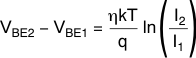
The value η in Equation 1 is a characteristic of the particular transistor used for the remote channel. The power-on reset value for the TMP451 device is η = 1.008. The value in the η-factor correction register may be used to adjust the effective η-factor according to Equation 2 and Equation 3.
The η-factor correction value must be stored in twos complement format, yielding an effective data range from –128 to 127. The η-factor correction value is written to and read from pointer address 23h. The register power-on reset value is 00h, thus having no effect unless a different value is written to it.
Table 27. η-Factor Range
| NADJUST | η | ||
|---|---|---|---|
| BINARY | HEX | DECIMAL | |
| 0111 1111 | 7F | 127 | 0.950198 |
| 0000 1010 | 0A | 10 | 1.003195 |
| 0000 1000 | 08 | 8 | 1.004152 |
| 0000 0110 | 06 | 6 | 1.005111 |
| 0000 0100 | 04 | 4 | 1.006072 |
| 0000 0010 | 02 | 2 | 1.007035 |
| 0000 0001 | 01 | 1 | 1.007517 |
| 0000 0000 | 00 | 0 | 1.008 |
| 1111 1111 | FF | –1 | 1.008483 |
| 1111 1110 | FE | –2 | 1.008967 |
| 1111 1100 | FC | –4 | 1.009935 |
| 1111 1010 | FA | –6 | 1.010905 |
| 1111 1000 | F8 | –8 | 1.011877 |
| 1111 0110 | F6 | –10 | 1.012851 |
| 1000 0000 | 80 | –128 | 1.073837 |
7.6.1.24 Digital Filter Control Register (offset: Read = 24h; Write = 24h) [reset = 00h]
| 7 | 6 | 5 | 4 | 3 | 2 | 1 | 0 |
| RESERVED | DF1 | DF0 | |||||
| R/W-0h | R/W-0h | R/W-0h | |||||
| LEGEND: R/W = Read/Write; R = Read only; -n = value after reset |
Table 28. Digital Filter Control Register Field Descriptions
| Bit | Field | Type | Reset | Description |
|---|---|---|---|---|
| 1 - 0 | DF1 - DF0 | R/W | 0h |
Configures the amount of filtering for the remote temperature results. Refer toTable 29 |
Table 29. Digital Filter Configuration
| VALUE | Number of Remote Temperature Measurements Averaged |
|---|---|
| 0h | Averaging off |
| 1h | 4 |
| 2h | 8 |
| 4h | not used |
7.6.1.25 Manufacturer ID Register (offset: Read = FEh; Write = N/A) [reset = 55]
| 7 | 6 | 5 | 4 | 3 | 2 | 1 | 0 |
| ID7 | ID6 | ID5 | ID4 | ID3 | ID2 | ID1 | ID0 |
| R-0h | R-1h | R-0h | R-1h | R-0h | R-1h | R-0h | R-1h |
| LEGEND: R/W = Read/Write; R = Read only; -n = value after reset |
Table 30. Manufacturer ID Register Field Descriptions
| Bit | Field | Type | Reset | Description |
|---|---|---|---|---|
| 7 - 0 | ID7 - ID0 | R | 55h |
Manufacturer identification information |
The TMP451 device allows for the two-wire bus controller to query the device for manufacturer and device IDs to enable software identification of the device at the particular two-wire bus address. The manufacturer ID is obtained by reading from pointer address FEh. The TMP451 device reads 55h for the manufacturer code.