SBOS722B June 2015 – August 2016 TMP461
PRODUCTION DATA.
- 1 Features
- 2 Applications
- 3 Description
- 4 Simplified Block Diagram
- 5 Revision History
- 6 Pin Configuration and Functions
- 7 Specifications
-
8 Detailed Description
- 8.1 Overview
- 8.2 Functional Block Diagram
- 8.3 Feature Description
- 8.4 Device Functional Modes
- 8.5 Programming
- 8.6
Register Map
- 8.6.1
Register Information
- 8.6.1.1 Pointer Register
- 8.6.1.2 Local and Remote Temperature Registers
- 8.6.1.3 Status Register
- 8.6.1.4 Configuration Register
- 8.6.1.5 Conversion Rate Register
- 8.6.1.6 One-Shot Start Register
- 8.6.1.7 Channel Enable Register
- 8.6.1.8 Consecutive ALERT Register
- 8.6.1.9 η-Factor Correction Register
- 8.6.1.10 Remote Temperature Offset Register
- 8.6.1.11 Manufacturer Identification Register
- 8.6.1
Register Information
- 9 Application and Implementation
- 10Power Supply Recommendations
- 11Layout
- 12Device and Documentation Support
- 13Mechanical, Packaging, and Orderable Information
Package Options
Mechanical Data (Package|Pins)
- RUN|10
Thermal pad, mechanical data (Package|Pins)
- RUN|10
Orderable Information
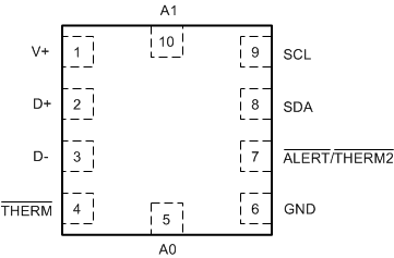
6 Pin Configuration and Functions
RUN Package
10-Pin WQFN
Top View

Pin Functions
| PIN | TYPE | DESCRIPTION | |
|---|---|---|---|
| NAME | NO. | ||
| A0 | 5 | Digital input | Address select. Connect to GND, V+, or leave floating. |
| A1 | 10 | Digital input | Address select. Connect to GND, V+, or leave floating. |
| ALERT/THERM2 | 7 | Digital output | Interrupt or SMBus alert output. Can be configured as a second THERM output. Open-drain; requires a pullup resistor to a voltage between 1.7 V and 3.6 V. |
| D– | 3 | Analog input | Negative connection to remote temperature sensor |
| D+ | 2 | Analog input | Positive connection to remote temperature sensor |
| GND | 6 | Ground | Supply ground connection |
| SCL | 9 | Digital input | Serial clock line for SMBus. Input; requires a pullup resistor to a voltage between 1.7 V and 3.6 V if driven by an open-drain output. |
| SDA | 8 | Bidirectional digital input-output | Serial data line for SMBus. Open-drain; requires a pullup resistor to a voltage between 1.7 V and 3.6 V. |
| THERM | 4 | Digital output | Thermal shutdown or fan-control pin. Open-drain; requires a pullup resistor to a voltage between 1.7 V and 3.6 V. |
| V+ | 1 | Power supply | Positive supply voltage, 1.7 V to 3.6 V |