SBOS828 December 2016 TMP708-Q1
PRODUCTION DATA.
- 1 Features
- 2 Applications
- 3 Description
- 4 Revision History
- 5 Pin Configuration and Functions
- 6 Specifications
- 7 Detailed Description
- 8 Application and Implementation
- 9 Power Supply Recommendations
- 10Layout
- 11Device and Documentation Support
- 12Mechanical, Packaging, and Orderable Information
Package Options
Mechanical Data (Package|Pins)
- DBV|5
Thermal pad, mechanical data (Package|Pins)
Orderable Information
10 Layout
10.1 Layout Guidelines
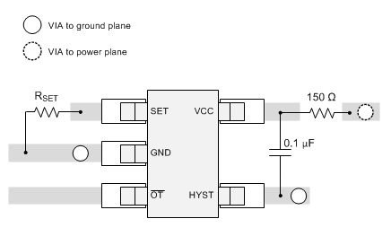
The TMP708-Q1 is extremely simple to lay out. Figure 7 shows the recommended board layout.
10.2 Layout Example
 Figure 7. Recommended Layout
10.3 Thermal Considerations
The TMP708-Q1 quiescent current is typically 40 μA. The device dissipates negligible power when the output drives a high-impedance load. Thus, the die temperature is the same as the package temperature. In order to maintain accurate temperature monitoring, provide a good thermal contact between the TMP708-Q1 package and the device being monitored. The rise in die temperature as a result of self-heating is given by Equation 2:
Equation 2. ΔTJ = PDISS × θJA
where
- PDISS = power dissipated by the device.
- θJA = package thermal resistance. Typical thermal resistance for SOT-23 package is 217.9°C/W.
To limit the effects of self-heating, keep the output current at a minimum level.