SBOS840 November   2016 TMP75C-Q1

PRODUCTION DATA.  

  1. Features
  2. Applications
  3. Description
  4. Revision History
  5. Pin Configuration and Functions
  6. Specifications
    1. 6.1 Absolute Maximum Ratings
    2. 6.2 ESD Ratings
    3. 6.3 Recommended Operating Conditions
    4. 6.4 Thermal Information
    5. 6.5 Electrical Characteristics
    6. 6.6 Typical Characteristics
  7. Detailed Description
    1. 7.1 Overview
    2. 7.2 Functional Block Diagram
    3. 7.3 Feature Description
      1. 7.3.1 Digital Temperature Output
      2. 7.3.2 Temperature Limits and Alert
      3. 7.3.3 Serial Interface
        1. 7.3.3.1 Bus Overview
        2. 7.3.3.2 Serial Bus Address
        3. 7.3.3.3 Writing and Reading Operation
        4. 7.3.3.4 Slave Mode Operations
          1. 7.3.3.4.1 Slave Receiver Mode:
          2. 7.3.3.4.2 Slave Transmitter Mode:
        5. 7.3.3.5 High-Speed (Hs) Mode
        6. 7.3.3.6 Timeout Function
        7. 7.3.3.7 Two-Wire Timing
        8. 7.3.3.8 Two-Wire Timing Diagrams
    4. 7.4 Device Functional Modes
      1. 7.4.1 Continuous-Conversion Mode
      2. 7.4.2 Shutdown Mode
      3. 7.4.3 One-Shot Mode
    5. 7.5 Programming
    6. 7.6 Register Map
  8. Application and Implementation
    1. 8.1 Application Information
    2. 8.2 Typical Application
      1. 8.2.1 Design Requirements
      2. 8.2.2 Detailed Design Procedure
      3. 8.2.3 Application Curves
  9. Power Supply Recommendations
  10. 10Layout
    1. 10.1 Layout Guidelines
    2. 10.2 Layout Example
  11. 11Device and Documentation Support
    1. 11.1 Documentation Support
      1. 11.1.1 Related Documentation
    2. 11.2 Receiving Notification of Documentation Updates
    3. 11.3 Community Resources
    4. 11.4 Trademarks
    5. 11.5 Electrostatic Discharge Caution
    6. 11.6 Glossary
  12. 12Mechanical, Packaging, and Orderable Information

Package Options

Mechanical Data (Package|Pins)
Thermal pad, mechanical data (Package|Pins)
Orderable Information

Pin Configuration and Functions

D and DGK Packages
8-Pin SOIC and VSSOP
Top View
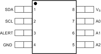
TMP75C-Q1 po_soic_sbos706.gif

Pin Functions

PIN I/O DESCRIPTION
NAME NO.
A0 7 I Address select. Connect to GND or VS.
A1 6 I Address select. Connect to GND or VS.
A2 5 I Address select. Connect to GND or VS.
ALERT 3 O Overtemperature alert. Open-drain output; requires a pull-up resistor.
GND 4 Ground.
SCL 2 I Serial clock.
SDA 1 I/O Serial data. Open-drain output; requires a pull-up resistor.
VS 8 I Supply voltage, 1.4 V to 3.6 V.