SCDS382C April 2018 – August 2019 TMUX1072
PRODUCTION DATA.
- 1 Features
- 2 Applications
- 3 Description
- 4 Revision History
- 5 Pin Configuration and Functions
- 6 Specifications
- 7 Parameter Measurement Information
- 8 Detailed Description
- 9 Application and Implementation
- 10Power Supply Recommendations
- 11Layout
- 12Device and Documentation Support
- 13Mechanical, Packaging, and Orderable Information
Package Options
Mechanical Data (Package|Pins)
Thermal pad, mechanical data (Package|Pins)
Orderable Information
7 Parameter Measurement Information
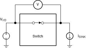
Channel ON, RON = V/ISINK
Figure 4. ON-State Resistance (RON) 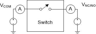 Figure 5. Off Leakage
 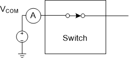 Figure 6. On Leakage
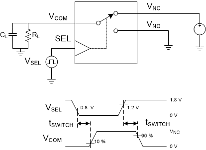
1. All input pulses are supplied by generators having the following characteristics: PRR ≤ 10 MHz, ZO = 50 Ω, tr < 500 ps, tf < 500 ps.
2. CL includes probe and jig capacitance.
Figure 7. tSWITCH Timing 
1. All input pulses are supplied by generators having the following characteristics: PRR ≤ 10 MHz, ZO = 50 Ω, tr < 500 ps, tf < 500 ps.
2. CL includes probe and jig capacitance.
Figure 8. tON, tOFF for OE 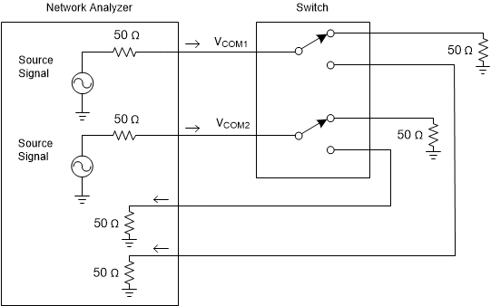 Figure 9. Off Isolation
 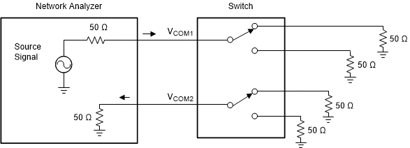 Figure 10. Cross Talk
 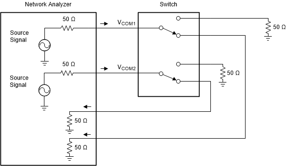 Figure 11. BW and Insertion Loss
  Figure 12. tEN_OVP and tDIS_OVP Timing Diagram
1. All input pulses are supplied by generators having the following characteristics: PRR ≤ 10 MHz, ZO = 50 Ω, tr < 500 ps, tf < 500 ps.
2. CL includes probe and jig capacitance.
Figure 13. tPD 
1. All input pulses are supplied by generators having the following characteristics: PRR ≤ 10 MHz, ZO = 50 Ω, tr < 500 ps, tf < 500 ps.
2. CL includes probe and jig capacitance.
Figure 14. tSK