SCDS392C November 2018 – February 2024 TMUX1104
PRODUCTION DATA
- 1
- 1 Features
- 2 Applications
- 3 Description
- 4 Pin Configuration and Functions
-
5 Specifications
- 5.1 Absolute Maximum Ratings
- 5.2 ESD Ratings
- 5.3 Recommended Operating Conditions
- 5.4 Thermal Information
- 5.5 Electrical Characteristics (VDD = 5V ±10 %)
- 5.6 Electrical Characteristics (VDD = 3.3V ±10 %)
- 5.7 Electrical Characteristics (VDD = 1.8V ±10 %)
- 5.8 Electrical Characteristics (VDD = 1.2V ±10 %)
- 5.9 Typical Characteristics
- 6 Parameter Measurement Information
- 7 Detailed Description
- 8 Application and Implementation
- 9 Device and Documentation Support
- 10Revision History
- 11Mechanical, Packaging, and Orderable Information
Package Options
Refer to the PDF data sheet for device specific package drawings
Mechanical Data (Package|Pins)
- DGS|10
- DQA|10
Thermal pad, mechanical data (Package|Pins)
- DQA|10
Orderable Information
3 Description
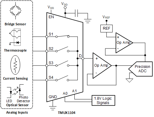
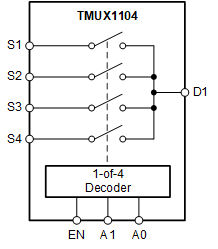
The TMUX1104 is a precision complementary metal-oxide semiconductor (CMOS) multiplexer (MUX). The TMUX1104 offers a single channel, 4:1 configuration. A wide operating supply of 1.08V to 5.5V makes this device an excellent choice for a broad array of applications from medical equipment to industrial systems. The device supports bidirectional analog and digital signals on the source (Sx) and drain (D) pins ranging from GND to VDD. All logic inputs have 1.8V logic compatible thresholds, allowing for both TTL and CMOS logic compatibility when operating in the valid supply voltage range. Fail-Safe Logic circuitry allows voltages on the control pins to be applied before the supply pin, protecting the device from potential damage.
The TMUX1104 is part of the precision switches and multiplexers family of devices. These devices have very low on and off leakage currents and low charge injection, allowing them to be used in high precision measurement applications. A low supply current of 5nA and small package options enable use in portable applications.
| PART NUMBER | PACKAGE(1) | PACKAGE SIZE(2) |
|---|---|---|
| TMUX1104 | DGS (VSSOP, 10) | 3mm × 4.9mm |
| DQA (USON, 10) | 2.5mm × 1mm |
 Simplified Schematic
 Block Diagram