SCDS400B march 2022 – july 2023 TMUX7348F , TMUX7349F
PRODMIX
- 1
- 1 Features
- 2 Applications
- 3 Description
- 4 Revision History
- 5 Device Comparison Table
- 6 Pin Configuration and Functions
-
7 Specifications
- 7.1 Absolute Maximum Ratings
- 7.2 ESD Ratings
- 7.3 Thermal Information
- 7.4 Recommended Operating Conditions
- 7.5 Electrical Characteristics (Global)
- 7.6 ±15 V Dual Supply: Electrical Characteristics
- 7.7 ±20 V Dual Supply: Electrical Characteristics
- 7.8 12 V Single Supply: Electrical Characteristics
- 7.9 36 V Single Supply: Electrical Characteristics
- 7.10 Typical Characteristics
-
8 Parameter Measurement Information
- 8.1 On-Resistance
- 8.2 Off-Leakage Current
- 8.3 On-Leakage Current
- 8.4 Input and Output Leakage Current Under Overvoltage Fault
- 8.5 Break-Before-Make Delay
- 8.6 Enable Delay Time
- 8.7 Transition Time
- 8.8 Fault Response Time
- 8.9 Fault Recovery Time
- 8.10 Fault Flag Response Time
- 8.11 Fault Flag Recovery Time
- 8.12 Charge Injection
- 8.13 Off Isolation
- 8.14 Crosstalk
- 8.15 Bandwidth
- 8.16 THD + Noise
-
9 Detailed Description
- 9.1 Overview
- 9.2 Functional Block Diagram
- 9.3 Feature Description
- 9.4 Device Functional Modes
- 10Application and Implementation
- 11Device and Documentation Support
- 12Mechanical, Packaging, and Orderable Information
Package Options
Mechanical Data (Package|Pins)
Thermal pad, mechanical data (Package|Pins)
Orderable Information
9.3.2.8 EMC Protection
The TMUX7348F and TMUX7349F are not intended for standalone electromagnetic compatibility (EMC) protection in industrial applications. There are three common high voltage transient specifications that govern industrial high voltage transient specifications: IEC61000-4-2 (ESD), IEC61000-4-4 (EFT), and IEC61000-4-5 (surge immunity). A transient voltage suppressor (TVS), along with some low-value series current limiting resistors, are required to prevent source input voltages from going above the rated ±60 V limits.
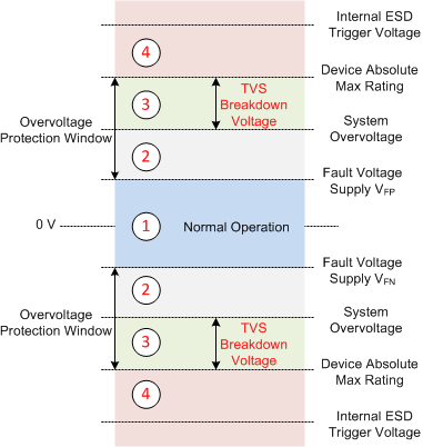
When selecting a TVS protection device, it is critical to ensure that the maximum working voltage is greater than both the normal operating range of the input source pins to be protected and any known system common-mode overvoltage that may be present due to incorrect wiring, loss of power, or short circuit. Figure 9-2 shows an example of the proper design window when selecting a TVS device.
Region 1 denotes the normal operation region of TMUX7348F and TMUX7349F where the input source voltages stay below the fault supplies VFP and VFN. Region 2 represents the range of possible persistent DC (or long duration AC overvoltage fault) presented on the source input pins. Region 3 represents the margin between any known DC overvoltage level and the absolute maximum rating of the TMUX7348F and TMUX7349F. The TVS breakdown voltage must be selected to be less than the absolute maximum rating of the TMUX7348F and TMUX7349F, but greater than any known possible persistent DC or long duration AC overvoltage fault to avoid triggering the TVS inadvertently. Region 4 represents the margin system designers must impose when selecting the TVS protection device to prevent accidental triggering of ESD cells of the TMUX7348F and TMUX7349F devices.
 Figure 9-2 System Operation Regions and Proper
Region of Selecting a TVS Protection Device