SCDS435B september 2021 – august 2023 TMUX8108 , TMUX8109
PRODUCTION DATA
- 1
- 1 Features
- 2 Applications
- 3 Description
- 4 Revision History
- 5 Device Comparison Table
- 6 Pin Configuration and Functions
-
7 Specifications
- 7.1 Absolute Maximum Ratings: TMUX810x Devices
- 7.2 ESD Ratings
- 7.3 Recommended Operating Conditions: TMUX810x Devices
- 7.4 Thermal Information
- 7.5 Electrical Characteristics (Global): TMUX810x Devices
- 7.6 Electrical Characteristics (±15-V Dual Supply)
- 7.7 Electrical Characteristics (±36-V Dual Supply)
- 7.8 Electrical Characteristics (±50-V Dual Supply)
- 7.9 Electrical Characteristics (72-V Single Supply)
- 7.10 Electrical Characteristics (100-V Single Supply)
- 7.11 Switching Characteristics: TMUX810x Devices
- 7.12 Typical Characteristics
- 8 Parameter Measurement Information
- 9 Detailed Description
- 10Application and Implementation
- 11Device and Documentation Support
- 12Mechanical, Packaging, and Orderable Information
Package Options
Refer to the PDF data sheet for device specific package drawings
Mechanical Data (Package|Pins)
- PW|16
- RUM|16
Thermal pad, mechanical data (Package|Pins)
- RUM|16
Orderable Information
3 Description
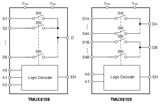
The TMUX8108 and TMUX8109 are modern high voltage capable analog multiplexers in 8:1 (single ended) and 4:1 (differential) configurations. The devices work well with dual supplies, a single supply, or asymmetric supplies up to a maximum supply voltage of 100 V. The TMUX810x devices provide consistent analog parametric performance across the entire supply voltage range. The TMUX8108 and TMUX8109 support bidirectional analog and digital signals on the source (Sx) and drain (Dx) pins.
All logic inputs support logic levels of 1.8 V, 3.3 V, 5V and can be connected as high as 48 V, allowing for system flexibility with control signal voltage. Fail-safe logic circuitry allows voltages on the logic pins to be applied before the supply pin, protecting the device from potential damage.
The device family provides latch-up immunity, preventing undesirable high current events between parasitic structures within the device. A latch-up condition typically continues until the power supply rails are turned off and can lead to device failure. The latch-up immunity feature allows this family of multiplexers to be used in harsh environments.
| PART NUMBER(1) | PACKAGE(2) | PACKAGE SIZE(3) |
|---|---|---|
| TMUX8108 TMUX8109 | PW (TSSOP, 16) | 5 mm × 6.4 mm |
| RUM (WQFN, 16) | 4 mm × 4 mm |
 TMUX8108 and TMUX8109 Block Diagram